

Lihat spesifikasi untuk detail produk.
XC7S15-1FTGB196I
Product Overview
Category
XC7S15-1FTGB196I belongs to the category of Field-Programmable Gate Arrays (FPGAs).
Use
This product is primarily used in digital logic circuits and electronic systems for various applications.
Characteristics
- Programmable: The XC7S15-1FTGB196I is a programmable device that allows users to configure its internal logic according to their specific requirements.
- High Performance: It offers high-speed performance, making it suitable for applications that demand fast processing.
- Versatile: This FPGA can be used in a wide range of applications due to its flexibility and reconfigurability.
- Low Power Consumption: The XC7S15-1FTGB196I is designed to operate efficiently with low power consumption.
- Compact Package: It comes in a compact package, which makes it suitable for space-constrained designs.
- Robust Packaging: The device is packaged in a durable and reliable manner to ensure protection during handling and operation.
Specifications
- Model: XC7S15-1FTGB196I
- Logic Cells: 15,000
- Flip-Flops: 30,000
- Block RAM: 600 Kb
- DSP Slices: 40
- I/O Pins: 196
- Operating Voltage: 1.2V
- Maximum Frequency: 500 MHz
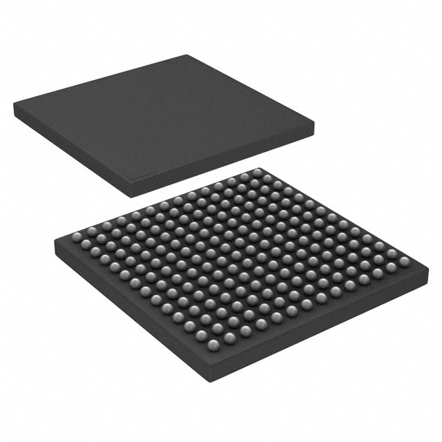
- Package Type: FTGB196
- Temperature Range: -40°C to +100°C
Pin Configuration
The detailed pin configuration of XC7S15-1FTGB196I can be found in the product datasheet or user manual provided by the manufacturer.
Functional Features
- Reconfigurability: The XC7S15-1FTGB196I can be reprogrammed multiple times, allowing for design changes and updates without the need for hardware modifications.
- High-Speed Processing: It offers fast processing capabilities, making it suitable for applications that require real-time data processing.
- Flexible I/O Options: The FPGA provides a large number of I/O pins, allowing for versatile connectivity options with other components or external devices.
- Embedded Memory: With its built-in block RAM, the XC7S15-1FTGB196I can efficiently store and retrieve data during operation.
- DSP Slices: The device includes dedicated digital signal processing (DSP) slices, enabling efficient implementation of complex algorithms.
Advantages
- Flexibility: The reconfigurable nature of FPGAs allows for quick prototyping and design iterations.
- Customization: Users can tailor the logic and functionality of the XC7S15-1FTGB196I to meet their specific requirements.
- High Performance: The FPGA's high-speed processing capability enables efficient execution of complex tasks.
- Low Power Consumption: The device operates with low power consumption, making it suitable for battery-powered applications.
Disadvantages
- Complexity: Utilizing FPGAs requires expertise in digital design and programming.
- Cost: FPGAs can be more expensive compared to fixed-function integrated circuits for certain applications.
- Limited Resources: The available logic cells, memory, and I/O pins may impose constraints on the complexity and scale of designs.
Working Principles
The XC7S15-1FTGB196I works based on the principle of configurable logic blocks (CLBs) and interconnects. These CLBs consist of look-up tables (LUTs), flip-flops, and multiplexers that can be programmed to implement desired logic functions. The interconnects allow for routing signals between different CLBs and I/O pins, enabling communication and data transfer within the FPGA.
Application Field Plans
The XC7S15-1FTGB196I finds applications in various fields, including: - Communications: It can be used in networking equipment, wireless communication systems, and data transmission devices. - Industrial Automation: The FPGA is suitable for control systems, robotics, and process automation applications. - Aerospace and Defense: It can be utilized in avionics, radar systems, and military-grade electronics. - Medical Devices: The XC7S15-1FTGB196I can be employed in medical imaging, patient monitoring, and diagnostic equipment. - Automotive Electronics: It finds use in automotive control systems, driver assistance systems, and infotainment systems.
Alternative Models
- XC7S25-1FTGB196I: A higher-capacity FPGA with 25,000 logic cells and additional features.
- XC7S6-1FTGB196I: A lower-capacity FPGA with 6,000 logic cells, suitable for smaller-scale designs.
- XC7S50-1FTGB196I: A higher-performance FPGA with 50,000 logic cells and enhanced capabilities.
These alternative models offer different capacities and features to cater to varying design requirements.
In conclusion, the XC7S15-
Sebutkan 10 pertanyaan dan jawaban umum terkait penerapan XC7S15-1FTGB196I dalam solusi teknis
Sure! Here are 10 common questions and answers related to the application of XC7S15-1FTGB196I in technical solutions:
Q1: What is XC7S15-1FTGB196I? A1: XC7S15-1FTGB196I is a specific model of Xilinx Spartan-7 FPGA (Field Programmable Gate Array) that offers 15,850 logic cells and various other features.
Q2: What are the key features of XC7S15-1FTGB196I? A2: Some key features of XC7S15-1FTGB196I include 15,850 logic cells, 900 Kbits of block RAM, 4 DSP slices, 100 MHz clock frequency, and support for various I/O standards.
Q3: What are the typical applications of XC7S15-1FTGB196I? A3: XC7S15-1FTGB196I is commonly used in applications such as industrial automation, automotive electronics, medical devices, communication systems, and consumer electronics.
Q4: How can XC7S15-1FTGB196I be programmed? A4: XC7S15-1FTGB196I can be programmed using Xilinx's Vivado Design Suite, which provides a comprehensive development environment for FPGA designs.
Q5: What are the power requirements for XC7S15-1FTGB196I? A5: XC7S15-1FTGB196I typically requires a supply voltage of 1.2V and consumes power based on the design complexity and operating conditions.
Q6: Can XC7S15-1FTGB196I interface with external devices? A6: Yes, XC7S15-1FTGB196I supports various I/O standards and can interface with external devices such as sensors, memory modules, communication interfaces, and other peripherals.
Q7: What are the available communication interfaces on XC7S15-1FTGB196I? A7: XC7S15-1FTGB196I provides multiple communication interfaces, including UART (Universal Asynchronous Receiver-Transmitter), SPI (Serial Peripheral Interface), I2C (Inter-Integrated Circuit), and GPIO (General Purpose Input/Output).
Q8: Can XC7S15-1FTGB196I be used for real-time signal processing? A8: Yes, XC7S15-1FTGB196I includes DSP slices that can be utilized for real-time signal processing tasks such as filtering, modulation, demodulation, and digital signal processing algorithms.
Q9: Is XC7S15-1FTGB196I suitable for low-power applications? A9: XC7S15-1FTGB196I is designed to offer a balance between performance and power consumption. However, for ultra-low-power applications, other FPGA families or specialized low-power devices may be more suitable.
Q10: Are there any development boards available for XC7S15-1FTGB196I? A10: Yes, Xilinx offers development boards like the Arty S7-25T, which features XC7S15-1FTGB196I, allowing users to prototype and develop their designs using this FPGA.
Please note that these answers are general and may vary depending on specific design requirements and application scenarios.