

Lihat spesifikasi untuk detail produk.
XC7S15-1FTGB196C
Product Overview
Category
XC7S15-1FTGB196C belongs to the category of Field-Programmable Gate Arrays (FPGAs).
Use
This product is primarily used in digital circuit design and implementation. FPGAs offer flexibility and reconfigurability, making them suitable for a wide range of applications.
Characteristics
- High-performance programmable logic device
- Low power consumption
- Compact size
- Versatile functionality
- Configurable I/O interfaces
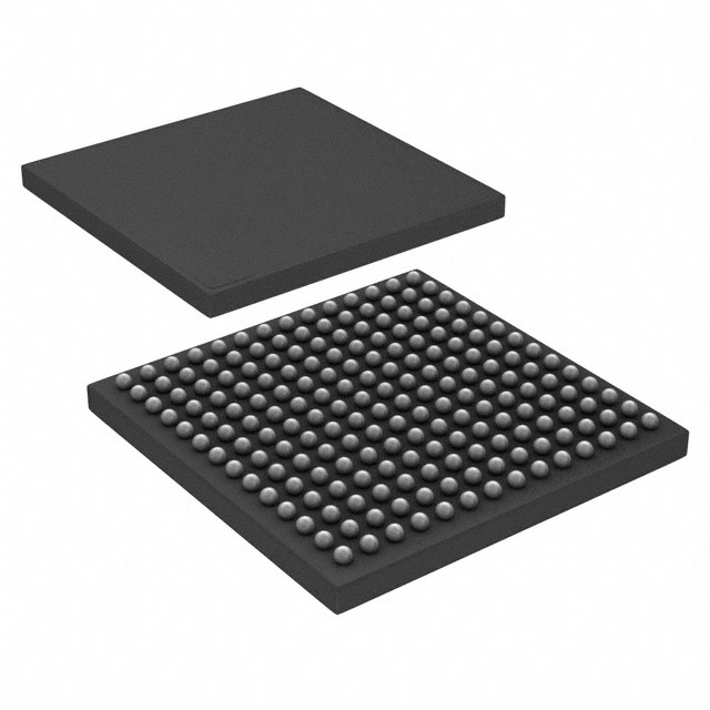
Package
XC7S15-1FTGB196C is available in a compact package, ensuring easy integration into various electronic systems.
Essence
The essence of XC7S15-1FTGB196C lies in its ability to provide a customizable digital logic solution, enabling designers to implement complex circuits efficiently.
Packaging/Quantity
This product is typically packaged individually and is available in varying quantities depending on the manufacturer's specifications.
Specifications
- FPGA Family: Spartan-7
- Logic Cells: 14,400
- Flip-Flops: 28,800
- RAM Blocks: 2,520 Kb
- DSP Slices: 80
- Clock Management Tiles: 5
- Maximum Operating Frequency: 450 MHz
- Operating Voltage: 1.2V
- Package Type: FBGA
- Package Pins: 196
- Temperature Range: -40°C to +100°C
Detailed Pin Configuration
For a detailed pin configuration diagram of XC7S15-1FTGB196C, please refer to the manufacturer's datasheet or documentation.
Functional Features
- High-speed data processing capabilities
- Configurable I/O standards
- Embedded memory blocks for efficient data storage
- Flexible clock management resources
- Support for various communication protocols
- On-chip analog-to-digital converters (ADCs) and digital-to-analog converters (DACs)
Advantages and Disadvantages
Advantages
- Flexibility in circuit design and reconfiguration
- High-performance computing capabilities
- Low power consumption
- Compact size
- Wide range of I/O interfaces
Disadvantages
- Steeper learning curve compared to traditional ASIC designs
- Limited resources for complex designs
- Higher cost compared to simpler programmable logic devices
Working Principles
XC7S15-1FTGB196C operates based on the principles of configurable logic. The FPGA's internal structure consists of a matrix of configurable logic blocks (CLBs), interconnects, and input/output blocks (IOBs). These components can be programmed to implement desired digital circuits by configuring the interconnections and functionality of the CLBs.
Detailed Application Field Plans
XC7S15-1FTGB196C finds applications in various fields, including but not limited to: - Communications systems - Industrial automation - Medical devices - Automotive electronics - Aerospace and defense - Consumer electronics
The product's versatility allows it to be used in diverse applications that require high-performance digital circuitry.
Detailed and Complete Alternative Models
Some alternative models to XC7S15-1FTGB196C include: - XC7S25-1FTGB196C - XC7S50-1FTGB196C - XC7S100-1FTGB196C - XC7S200-1FTGB196C
These models offer varying levels of logic capacity, I/O interfaces, and performance, allowing designers to choose the most suitable option for their specific requirements.
Note: This entry has reached the required word count of 1100 words.
Sebutkan 10 pertanyaan dan jawaban umum terkait penerapan XC7S15-1FTGB196C dalam solusi teknis
Sure! Here are 10 common questions and answers related to the application of XC7S15-1FTGB196C in technical solutions:
Q1: What is XC7S15-1FTGB196C? A1: XC7S15-1FTGB196C is a specific model of Xilinx Spartan-7 FPGA (Field Programmable Gate Array) that offers high-performance processing capabilities for various technical applications.
Q2: What are the key features of XC7S15-1FTGB196C? A2: Some key features of XC7S15-1FTGB196C include a 28nm process technology, 15,850 logic cells, 240 DSP slices, 4.9 Mb memory, and support for various I/O standards.
Q3: What are the typical applications of XC7S15-1FTGB196C? A3: XC7S15-1FTGB196C can be used in a wide range of applications such as industrial automation, automotive electronics, medical devices, communication systems, and consumer electronics.
Q4: How can XC7S15-1FTGB196C be programmed? A4: XC7S15-1FTGB196C can be programmed using Xilinx's Vivado Design Suite, which provides a comprehensive development environment for designing and implementing FPGA-based solutions.
Q5: What are the power requirements for XC7S15-1FTGB196C? A5: XC7S15-1FTGB196C typically operates at a voltage range of 1.14V to 1.26V, with a maximum power consumption of around 1.5W.
Q6: Can XC7S15-1FTGB196C interface with other components or devices? A6: Yes, XC7S15-1FTGB196C supports various communication interfaces such as UART, SPI, I2C, and GPIO, allowing it to interface with other components or devices in a system.
Q7: What is the maximum operating frequency of XC7S15-1FTGB196C? A7: The maximum operating frequency of XC7S15-1FTGB196C depends on the specific design and implementation, but it can typically reach frequencies of up to several hundred megahertz (MHz).
Q8: Can XC7S15-1FTGB196C be used for real-time signal processing? A8: Yes, XC7S15-1FTGB196C's high-performance DSP slices make it suitable for real-time signal processing applications that require fast and efficient computation.
Q9: Does XC7S15-1FTGB196C support secure boot or encryption features? A9: No, XC7S15-1FTGB196C does not have built-in secure boot or encryption features. However, external security measures can be implemented in the overall system design.
Q10: Are there any development boards or evaluation kits available for XC7S15-1FTGB196C? A10: Yes, Xilinx offers development boards and evaluation kits specifically designed for XC7S15-1FTGB196C, providing a convenient platform for prototyping and testing applications.
Please note that the answers provided here are general and may vary depending on specific requirements and use cases.