

Lihat spesifikasi untuk detail produk.
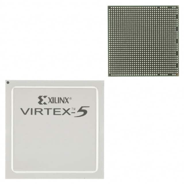
XC5VSX35T-1FF665I
Product Overview
Category
XC5VSX35T-1FF665I belongs to the category of Field Programmable Gate Arrays (FPGAs).
Use
FPGAs are integrated circuits that can be programmed and reprogrammed to perform various digital functions. They are widely used in industries such as telecommunications, automotive, aerospace, and consumer electronics.
Characteristics
- High flexibility: FPGAs can be customized to perform specific tasks by programming their internal logic.
- Parallel processing: FPGAs can execute multiple operations simultaneously, leading to improved performance.
- Reconfigurability: FPGAs can be reprogrammed multiple times, allowing for design changes and updates.
- Low power consumption: FPGAs offer efficient power usage compared to other programmable devices.
- High-speed operation: FPGAs can process data at high speeds, making them suitable for real-time applications.
Package and Quantity
XC5VSX35T-1FF665I is available in a specific package type known as Flip-Chip FineLine BGA (Ball Grid Array). It is typically sold individually or in small quantities.
Specifications
- FPGA Family: Virtex-5
- Logic Cells: 33,280
- Slices: 2,080
- DSP48A1 Slices: 20
- Block RAM: 1,728 Kb
- Maximum Number of User I/Os: 665
- Operating Voltage: 1.2V
- Operating Temperature Range: -40°C to +100°C
- Package Type: Flip-Chip FineLine BGA
- Package Pins: 665
- Package Dimensions: 27mm x 27mm
Detailed Pin Configuration
The XC5VSX35T-1FF665I FPGA has a total of 665 pins, each serving a specific purpose. The pin configuration includes input/output pins, clock pins, power supply pins, and configuration pins. A detailed pinout diagram can be found in the product datasheet.
Functional Features
XC5VSX35T-1FF665I offers several functional features that make it suitable for a wide range of applications:
- High-speed serial connectivity: The FPGA supports various high-speed serial protocols such as PCIe, SATA, and Gigabit Ethernet.
- Embedded processing capabilities: It includes PowerPC 440 microprocessors for implementing complex algorithms and control functions.
- Integrated memory resources: The FPGA incorporates large on-chip memory blocks for efficient data storage and retrieval.
- Flexible I/O standards: It supports multiple I/O standards, including LVCMOS, LVTTL, and differential signaling standards like LVDS and LVPECL.
- Advanced DSP capabilities: The FPGA includes dedicated digital signal processing (DSP) slices for performing complex mathematical operations efficiently.
Advantages and Disadvantages
Advantages
- Versatility: FPGAs can be programmed to perform a wide range of tasks, making them highly adaptable to different applications.
- Rapid prototyping: FPGAs enable quick development and testing of digital designs, reducing time-to-market.
- Cost-effective: FPGAs eliminate the need for custom ASICs, resulting in lower development costs for certain applications.
- Reconfigurability: FPGAs can be reprogrammed, allowing for design changes and updates without requiring hardware modifications.
Disadvantages
- Complexity: Designing and programming FPGAs require specialized knowledge and expertise.
- Limited performance compared to application-specific integrated circuits (ASICs) for certain applications.
- Higher power consumption compared to dedicated hardware solutions.
Working Principles
FPGAs consist of an array of configurable logic blocks (CLBs) interconnected through programmable routing resources. The CLBs contain look-up tables (LUTs) that can be programmed to implement desired logic functions. The interconnections between CLBs can be configured to establish data paths and control signals.
During operation, the FPGA is programmed with a specific configuration bitstream that defines the desired functionality. The internal connections and logic within the FPGA are then established based on this configuration, allowing it to perform the intended tasks.
Detailed Application Field Plans
XC5VSX35T-1FF665I finds applications in various fields, including:
- Telecommunications: Used for high-speed data processing, signal routing, and protocol conversion in network equipment.
- Automotive: Employed in advanced driver assistance systems (ADAS), engine control units (ECUs), and infotainment systems.
- Aerospace: Utilized in satellite communication systems, radar processing, and flight control systems.
- Consumer Electronics: Integrated into video processing devices, gaming consoles, and multimedia systems.
- Industrial Automation: Applied in robotics, machine vision systems, and process control.
Alternative Models
For those seeking alternative models, the following FPGAs can be considered:
- Xilinx Virtex-7 XC
Sebutkan 10 pertanyaan dan jawaban umum terkait penerapan XC5VSX35T-1FF665I dalam solusi teknis
Sure! Here are 10 common questions and answers related to the application of XC5VSX35T-1FF665I in technical solutions:
Q1: What is XC5VSX35T-1FF665I? A1: XC5VSX35T-1FF665I is a specific model of Xilinx Virtex-5 FPGA (Field-Programmable Gate Array) that offers high-performance processing capabilities for various technical applications.
Q2: What are the key features of XC5VSX35T-1FF665I? A2: Some key features of XC5VSX35T-1FF665I include 35,200 logic cells, 1,344 Kb block RAM, 128 DSP slices, and support for various I/O standards.
Q3: What are the typical applications of XC5VSX35T-1FF665I? A3: XC5VSX35T-1FF665I is commonly used in applications such as telecommunications, aerospace, defense, industrial automation, and high-performance computing.
Q4: How can XC5VSX35T-1FF665I be programmed? A4: XC5VSX35T-1FF665I can be programmed using Xilinx's Vivado Design Suite or ISE Design Suite software tools, which allow users to design and implement their custom logic circuits.
Q5: What is the maximum operating frequency of XC5VSX35T-1FF665I? A5: The maximum operating frequency of XC5VSX35T-1FF665I depends on the specific design and implementation, but it can typically reach frequencies of several hundred megahertz.
Q6: Can XC5VSX35T-1FF665I interface with other components or devices? A6: Yes, XC5VSX35T-1FF665I supports various communication interfaces such as PCIe, Ethernet, USB, and serial protocols, allowing it to interface with other components or devices.
Q7: What are the power requirements for XC5VSX35T-1FF665I? A7: XC5VSX35T-1FF665I requires a supply voltage of 1.0V and has different power rails for core and I/O voltages. The specific power requirements can be found in the datasheet provided by Xilinx.
Q8: Can XC5VSX35T-1FF665I be used in safety-critical applications? A8: Yes, XC5VSX35T-1FF665I can be used in safety-critical applications, but additional measures may need to be taken to ensure functional safety, such as redundancy or fault-tolerant design techniques.
Q9: Are there any limitations or considerations when using XC5VSX35T-1FF665I? A9: Some considerations include power consumption, thermal management, and the need for proper signal integrity and timing analysis during the design phase. The datasheet and application notes from Xilinx provide more detailed information.
Q10: Where can I find technical support or documentation for XC5VSX35T-1FF665I? A10: Xilinx provides comprehensive technical support through their website, including documentation, application notes, forums, and direct contact with their support team.