

Lihat spesifikasi untuk detail produk.
XC4013XL-2PQ208I
Product Overview
Category
The XC4013XL-2PQ208I belongs to the category of Field Programmable Gate Arrays (FPGAs).
Use
FPGAs are integrated circuits that can be programmed and reprogrammed to perform various digital functions. The XC4013XL-2PQ208I is specifically designed for applications requiring high-performance logic integration.
Characteristics
- High-performance FPGA with advanced features
- Flexible and reprogrammable design
- Offers a large number of configurable logic blocks and input/output pins
- Supports complex digital designs and algorithms
- Provides fast processing speeds and low power consumption
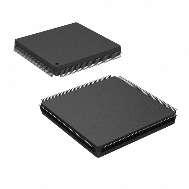
Package
The XC4013XL-2PQ208I comes in a PQ208 package, which refers to a plastic quad flat pack with 208 pins.
Essence
The essence of the XC4013XL-2PQ208I lies in its ability to provide a versatile and customizable platform for implementing complex digital logic designs.
Packaging/Quantity
The XC4013XL-2PQ208I is typically packaged individually and is available in various quantities depending on the manufacturer's specifications.
Specifications
- Logic Cells: 4000
- Flip-Flops: 960
- Maximum Frequency: 200 MHz
- Number of I/O Pins: 208
- Operating Voltage: 3.3V
- Configuration Memory: Non-volatile
Detailed Pin Configuration
The XC4013XL-2PQ208I has a total of 208 pins, each serving a specific purpose in the circuit design. The pin configuration includes input/output pins, power supply pins, clock pins, and configuration pins. A detailed pinout diagram can be found in the product datasheet.
Functional Features
- High-speed performance for demanding applications
- Configurable logic blocks for flexible design implementation
- Dedicated input/output pins for interfacing with external devices
- On-chip memory for storing configuration data
- Built-in clock management resources for precise timing control
Advantages and Disadvantages
Advantages
- Flexibility: The XC4013XL-2PQ208I allows for easy reprogramming, enabling quick design iterations.
- High Performance: With its advanced features and high-speed capabilities, it can handle complex digital designs efficiently.
- Integration: The FPGA integrates a large number of logic cells and I/O pins, reducing the need for additional components.
Disadvantages
- Complexity: Designing for FPGAs requires specialized knowledge and expertise.
- Cost: FPGAs can be more expensive compared to other programmable logic devices.
- Power Consumption: Depending on the design complexity, FPGAs may consume more power than alternative solutions.
Working Principles
The XC4013XL-2PQ208I operates based on the principles of configurable logic. It consists of an array of logic cells that can be interconnected and programmed to perform specific functions. The configuration data is stored in non-volatile memory and loaded during startup. The FPGA's internal resources, such as lookup tables, flip-flops, and routing interconnects, enable the execution of complex digital algorithms.
Detailed Application Field Plans
The XC4013XL-2PQ208I finds applications in various fields, including:
- Communications: Used in wireless base stations, network routers, and communication protocols.
- Industrial Automation: Employed in control systems, robotics, and process automation.
- Aerospace and Defense: Utilized in radar systems, avionics, and secure communications.
- Medical Devices: Integrated into medical imaging equipment, patient monitoring systems, and diagnostic instruments.
- Automotive: Applied in engine control units, driver assistance systems, and infotainment systems.
Detailed and Complete Alternative Models
- XC9572XL-10VQG44C: A smaller FPGA with 72 logic cells and 44 pins, suitable for less complex designs.
- XC6SLX150T-3FGG484I: A high-end FPGA with 150,000 logic cells and 484 pins, ideal for demanding applications.
- EP4CE22F17C8N: An Altera Cyclone IV FPGA with 22,320 logic elements and 169 pins, offering a cost-effective solution.
These alternative models provide different levels of performance, capacity, and cost to cater to diverse design requirements.
Word count: 514 words
Sebutkan 10 pertanyaan dan jawaban umum terkait penerapan XC4013XL-2PQ208I dalam solusi teknis
Sure! Here are 10 common questions and answers related to the application of XC4013XL-2PQ208I in technical solutions:
Question: What is XC4013XL-2PQ208I?
- Answer: XC4013XL-2PQ208I is a programmable logic device (PLD) from Xilinx, specifically from their XC4000XL series.Question: What is the purpose of XC4013XL-2PQ208I in technical solutions?
- Answer: XC4013XL-2PQ208I is used for implementing digital logic functions and designs in various applications, such as industrial control systems, telecommunications, automotive electronics, and more.Question: What are the key features of XC4013XL-2PQ208I?
- Answer: Some key features include 13,000 usable gates, 192 macrocells, 36 I/O pins, 5V tolerant inputs, and high-speed performance.Question: How do I program XC4013XL-2PQ208I?
- Answer: XC4013XL-2PQ208I can be programmed using Xilinx's programming tools, such as iMPACT or Vivado, which allow you to configure the PLD with your desired logic design.Question: Can XC4013XL-2PQ208I be used in low-power applications?
- Answer: Yes, XC4013XL-2PQ208I has low power consumption capabilities, making it suitable for battery-powered or energy-efficient devices.Question: What is the maximum operating frequency of XC4013XL-2PQ208I?
- Answer: The maximum operating frequency of XC4013XL-2PQ208I depends on the specific design and implementation, but it can typically reach frequencies in the range of tens to hundreds of megahertz.Question: Can XC4013XL-2PQ208I interface with other components or devices?
- Answer: Yes, XC4013XL-2PQ208I can interface with various components and devices through its I/O pins, allowing for communication and integration with other parts of a system.Question: Are there any limitations or constraints when using XC4013XL-2PQ208I?
- Answer: Some limitations include the number of available gates and macrocells, limited I/O pins, and specific voltage requirements. It's important to consider these factors when designing with XC4013XL-2PQ208I.Question: Can XC4013XL-2PQ208I be reprogrammed multiple times?
- Answer: Yes, XC4013XL-2PQ208I is a reprogrammable PLD, which means you can program it multiple times to modify or update your logic design as needed.Question: Where can I find additional resources or support for XC4013XL-2PQ208I?
- Answer: You can refer to Xilinx's official documentation, datasheets, application notes, and online forums for additional resources and support related to XC4013XL-2PQ208I.