

Lihat spesifikasi untuk detail produk.
XC4010XL-3PQ100I
Product Overview
Category
The XC4010XL-3PQ100I belongs to the category of Field Programmable Gate Arrays (FPGAs).
Use
FPGAs are integrated circuits that can be programmed and reprogrammed to perform various digital functions. The XC4010XL-3PQ100I is specifically designed for applications requiring high-performance logic integration.
Characteristics
- High-performance logic integration
- Programmable and reprogrammable functionality
- Flexible and customizable design options
- Efficient power consumption
- Wide range of application possibilities
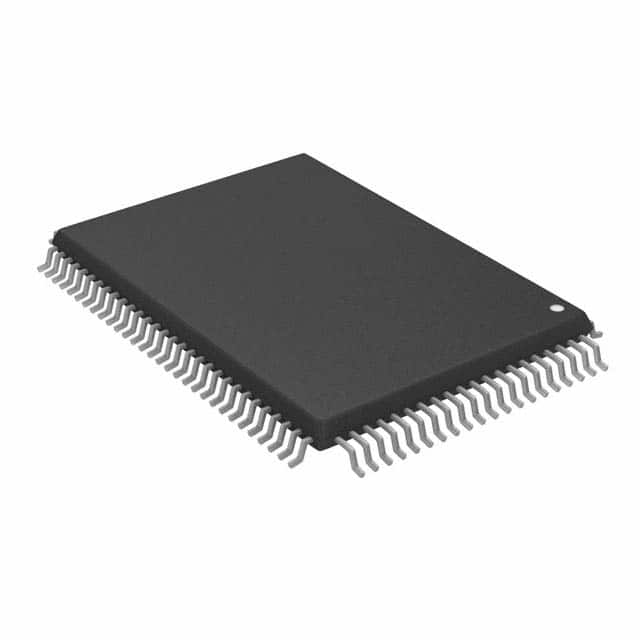
Package
The XC4010XL-3PQ100I comes in a PQ100 package, which refers to a plastic quad flat pack with 100 pins.
Essence
The essence of the XC4010XL-3PQ100I lies in its ability to provide a versatile and programmable solution for complex digital logic requirements.
Packaging/Quantity
The XC4010XL-3PQ100I is typically packaged in reels or trays, with each reel or tray containing a specific quantity of units. The exact packaging and quantity may vary depending on the supplier.
Specifications
- Logic Cells: 4000
- Maximum Frequency: 100 MHz
- Operating Voltage: 3.3V
- I/O Pins: 100
- Programmable Logic Blocks: 160
- RAM Bits: 32,768
- Flip-Flops: 4,096
- Configuration Memory: 10,000 bits
Detailed Pin Configuration
The XC4010XL-3PQ100I has a total of 100 pins, each serving a specific purpose in the overall functionality of the FPGA. The pin configuration includes input/output pins, power supply pins, clock pins, and configuration pins. A detailed pinout diagram can be found in the product datasheet.
Functional Features
- High-speed performance: The XC4010XL-3PQ100I offers fast processing capabilities, making it suitable for applications requiring real-time data processing.
- Flexibility: With its programmable nature, the FPGA allows for easy customization and adaptation to changing requirements.
- Integration: The XC4010XL-3PQ100I integrates a large number of logic cells, allowing for complex digital designs to be implemented on a single chip.
- Low power consumption: The FPGA is designed to optimize power usage, making it energy-efficient for various applications.
Advantages and Disadvantages
Advantages
- Versatility: The XC4010XL-3PQ100I can be programmed to perform a wide range of functions, making it suitable for diverse applications.
- Cost-effective: FPGAs eliminate the need for custom-designed ASICs, reducing development costs and time-to-market.
- Reconfigurability: The ability to reprogram the FPGA allows for design modifications without the need for hardware changes.
- Scalability: FPGAs can be easily scaled up or down depending on the complexity of the application.
Disadvantages
- Complexity: Programming and designing FPGAs require specialized knowledge and expertise.
- Limited performance optimization: Compared to dedicated hardware solutions, FPGAs may have slightly lower performance in certain applications.
- Higher power consumption: While FPGAs are generally power-efficient, they may consume more power compared to specific-purpose integrated circuits.
Working Principles
The XC4010XL-3PQ100I operates based on the principles of configurable logic. It consists of an array of programmable logic blocks interconnected through configurable routing resources. These logic blocks can be programmed to implement desired digital functions using Hardware Description Languages (HDL) such as VHDL or Verilog. The configuration memory stores the programming information, allowing the FPGA to be reprogrammed as needed.
Detailed Application Field Plans
The XC4010XL-3PQ100I finds applications in various fields, including:
- Communications: Used in wireless communication systems for signal processing and protocol implementation.
- Industrial Automation: Employed in control systems for real-time monitoring and automation of industrial processes.
- Aerospace and Defense: Utilized in radar systems, avionics, and military-grade communication equipment.
- Medical Devices: Integrated into medical imaging systems, patient monitoring devices, and diagnostic equipment.
- Automotive: Applied in advanced driver assistance systems (ADAS), engine control units (ECUs), and infotainment systems.
Detailed and Complete Alternative Models
- XC4028EX-4HQ240C: A higher-capacity FPGA with 4000 logic cells and 240 pins.
- XC9572XL-10VQG44C: A smaller FPGA with 72 logic cells and 44 pins, suitable for low-complexity applications.
- XC6SLX150-2FGG484I: A high-performance FPGA with 150,000 logic cells and
Sebutkan 10 pertanyaan dan jawaban umum terkait penerapan XC4010XL-3PQ100I dalam solusi teknis
Sure! Here are 10 common questions and answers related to the application of XC4010XL-3PQ100I in technical solutions:
Question: What is XC4010XL-3PQ100I?
Answer: XC4010XL-3PQ100I is a specific model of Field Programmable Gate Array (FPGA) manufactured by Xilinx.Question: What are the key features of XC4010XL-3PQ100I?
Answer: Some key features include 4000 logic cells, 64 I/O pins, 3.3V power supply, and a PQ100 package.Question: What are the typical applications of XC4010XL-3PQ100I?
Answer: XC4010XL-3PQ100I can be used in various applications such as digital signal processing, embedded systems, telecommunications, and industrial automation.Question: How does XC4010XL-3PQ100I differ from other FPGA models?
Answer: XC4010XL-3PQ100I has a specific combination of logic cells, I/O pins, voltage requirements, and package size that sets it apart from other FPGA models.Question: Can XC4010XL-3PQ100I be reprogrammed after deployment?
Answer: Yes, XC4010XL-3PQ100I is a field-programmable device, which means it can be reprogrammed even after it has been deployed in a system.Question: What programming languages can be used with XC4010XL-3PQ100I?
Answer: XC4010XL-3PQ100I can be programmed using Hardware Description Languages (HDLs) such as VHDL or Verilog.Question: What development tools are available for XC4010XL-3PQ100I?
Answer: Xilinx provides software tools like Vivado or ISE Design Suite that can be used for designing, simulating, and programming XC4010XL-3PQ100I.Question: Can XC4010XL-3PQ100I interface with other components or devices?
Answer: Yes, XC4010XL-3PQ100I can interface with various components and devices through its I/O pins, allowing it to communicate with sensors, actuators, memory modules, and more.Question: Are there any limitations or considerations when using XC4010XL-3PQ100I?
Answer: Some considerations include power supply requirements, heat dissipation, timing constraints, and the need for proper design verification and testing.Question: Where can I find additional resources or support for XC4010XL-3PQ100I?
Answer: You can refer to Xilinx's official website, user manuals, application notes, online forums, or seek assistance from Xilinx's technical support team for additional resources and support.
Please note that the answers provided here are general and may vary depending on specific requirements and use cases.