

Lihat spesifikasi untuk detail produk.
XC3S5000-4FGG900I
Product Overview
Category
XC3S5000-4FGG900I belongs to the category of Field-Programmable Gate Arrays (FPGAs).
Use
This product is primarily used in digital circuit design and implementation. FPGAs provide a flexible and customizable platform for designing and prototyping complex digital systems.
Characteristics
- High integration: XC3S5000-4FGG900I offers a large number of logic cells, allowing for the implementation of complex digital circuits.
- Programmability: The FPGA can be reprogrammed multiple times, enabling rapid prototyping and iterative design.
- Versatility: It supports a wide range of applications, from consumer electronics to industrial automation.
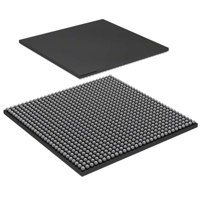
Package
XC3S5000-4FGG900I comes in a Fine-Pitch Ball Grid Array (FBGA) package.
Essence
The essence of XC3S5000-4FGG900I lies in its ability to provide a highly configurable and reprogrammable hardware platform for digital circuit design.
Packaging/Quantity
This product is typically packaged in trays or reels, with a quantity of 100 units per tray/reel.
Specifications
- Model: XC3S5000-4FGG900I
- Logic Cells: 5,000
- Operating Voltage: 1.2V
- Maximum Frequency: 400 MHz
- I/O Pins: 900
- Configuration Memory: 4 Mb
- Package Type: FBGA
- Temperature Range: -40°C to +85°C
Detailed Pin Configuration
The XC3S5000-4FGG900I has a total of 900 I/O pins, which are programmable and can be configured based on the specific requirements of the digital circuit being designed.
For a detailed pin configuration diagram, please refer to the product datasheet.
Functional Features
- High-speed performance: The XC3S5000-4FGG900I offers fast signal processing capabilities, making it suitable for applications that require high-speed data processing.
- Flexible I/O configuration: The programmable I/O pins allow for versatile connectivity options, enabling seamless integration with other components and systems.
- Embedded memory blocks: This FPGA includes dedicated memory blocks that can be used for storing data or implementing complex algorithms.
- Built-in DSP slices: The XC3S5000-4FGG900I features Digital Signal Processing (DSP) slices, which enable efficient implementation of mathematical operations commonly found in signal processing applications.
Advantages and Disadvantages
Advantages
- Flexibility: FPGAs offer a highly flexible platform for designing and prototyping digital circuits, allowing for rapid iterations and customization.
- Reconfigurability: The ability to reprogram the FPGA multiple times enables easy updates and modifications to the design without requiring hardware changes.
- High integration: With a large number of logic cells, the XC3S5000-4FGG900I can accommodate complex designs in a single chip.
Disadvantages
- Complexity: Designing for FPGAs requires specialized knowledge and expertise in digital circuit design.
- Power consumption: FPGAs tend to consume more power compared to application-specific integrated circuits (ASICs) for similar functionalities.
- Cost: FPGAs can be relatively expensive compared to other digital circuit implementation options.
Working Principles
The XC3S5000-4FGG900I operates based on the principles of configurable logic. It consists of an array of programmable logic cells interconnected through configurable routing resources. These logic cells can be programmed to implement various digital functions, such as logic gates, flip-flops, and arithmetic units. The configuration of the FPGA is stored in non-volatile memory, allowing for reprogramming as needed.
Detailed Application Field Plans
The XC3S5000-4FGG900I finds applications in various fields, including:
- Telecommunications: It can be used in the design of high-speed data communication systems, such as routers and switches.
- Industrial Automation: FPGAs are employed in industrial control systems to implement complex algorithms and interface with sensors and actuators.
- Automotive Electronics: They are utilized in automotive applications for functions like engine control, advanced driver assistance systems (ADAS), and infotainment systems.
- Aerospace and Defense: FPGAs play a crucial role in radar systems, avionics, and military-grade communication equipment.
- Consumer Electronics: They are used in devices like gaming consoles, digital cameras, and high-definition televisions for signal processing and multimedia applications.
Detailed and Complete Alternative Models
- XC3S2000-4FGG900I: A lower-capacity FPGA from the same family, offering 2,000 logic cells.
- XC3S1000-4FGG900I: Another variant with 1,
Sebutkan 10 pertanyaan dan jawaban umum terkait penerapan XC3S5000-4FGG900I dalam solusi teknis
Sure! Here are 10 common questions and answers related to the application of XC3S5000-4FGG900I in technical solutions:
Q: What is XC3S5000-4FGG900I? A: XC3S5000-4FGG900I is a field-programmable gate array (FPGA) from Xilinx, designed for high-performance applications.
Q: What are the key features of XC3S5000-4FGG900I? A: Some key features include a large number of logic cells, high-speed serial transceivers, embedded memory blocks, and advanced DSP capabilities.
Q: What are some typical applications of XC3S5000-4FGG900I? A: XC3S5000-4FGG900I is commonly used in applications such as telecommunications, aerospace, defense, industrial automation, and high-performance computing.
Q: How can I program XC3S5000-4FGG900I? A: XC3S5000-4FGG900I can be programmed using Xilinx's Vivado Design Suite or ISE Design Suite software tools.
Q: What is the maximum operating frequency of XC3S5000-4FGG900I? A: The maximum operating frequency of XC3S5000-4FGG900I depends on the specific design and implementation, but it can typically reach several hundred megahertz.
Q: Can XC3S5000-4FGG900I interface with other components or devices? A: Yes, XC3S5000-4FGG900I supports various standard interfaces such as PCIe, Ethernet, USB, SPI, I2C, and more, allowing it to communicate with other components or devices.
Q: What is the power consumption of XC3S5000-4FGG900I? A: The power consumption of XC3S5000-4FGG900I depends on the specific design and utilization, but it typically ranges from a few watts to tens of watts.
Q: Can XC3S5000-4FGG900I be used in safety-critical applications? A: Yes, XC3S5000-4FGG900I can be used in safety-critical applications by following appropriate design practices and adhering to relevant industry standards.
Q: Does XC3S5000-4FGG900I support partial reconfiguration? A: Yes, XC3S5000-4FGG900I supports partial reconfiguration, allowing specific sections of the FPGA to be reprogrammed while the rest of the design remains operational.
Q: Where can I find more information about XC3S5000-4FGG900I? A: You can find more detailed information about XC3S5000-4FGG900I in the official documentation provided by Xilinx, including datasheets, user guides, and application notes.
Please note that the answers provided here are general and may vary depending on the specific requirements and implementation of XC3S5000-4FGG900I in different technical solutions.