

Lihat spesifikasi untuk detail produk.
XC3S400A-4FGG400C
Product Overview
Category
XC3S400A-4FGG400C belongs to the category of Field-Programmable Gate Arrays (FPGAs).
Use
This product is primarily used in digital circuit design and implementation. FPGAs provide a flexible and customizable solution for various applications, including telecommunications, automotive, aerospace, and consumer electronics.
Characteristics
- High-performance: The XC3S400A-4FGG400C offers high-speed processing capabilities, making it suitable for demanding applications.
- Programmable: FPGAs can be reprogrammed multiple times, allowing for iterative design and easy modification.
- Versatile: This FPGA supports a wide range of functions and can be customized to meet specific requirements.
- Low power consumption: The XC3S400A-4FGG400C is designed to minimize power consumption, making it energy-efficient.
Package and Quantity
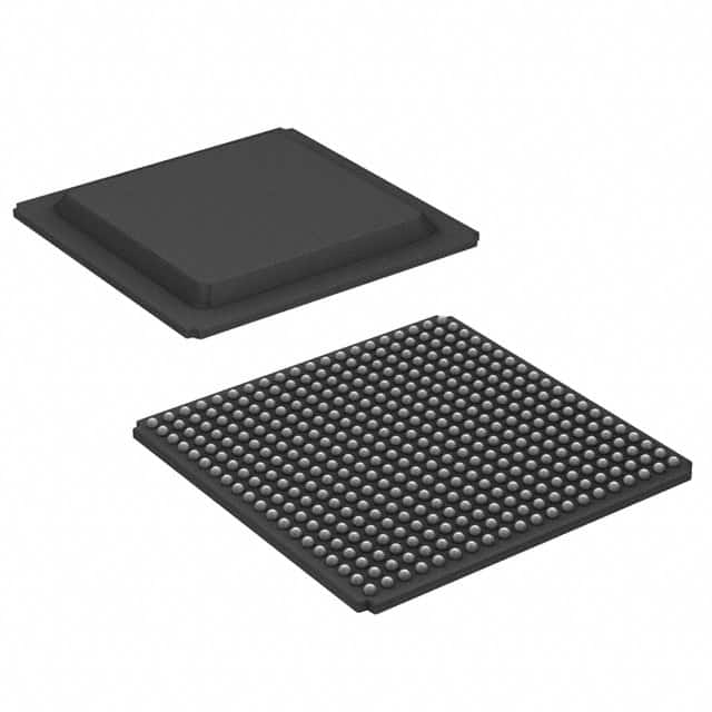
The XC3S400A-4FGG400C comes in a FG(G) package, which stands for Fine-Pitch Ball Grid Array. It contains 400 pins and is available in a quantity specified by the manufacturer.
Specifications
- Logic Cells: 400,000
- Block RAM: 1,728 Kbits
- DSP Slices: 192
- Maximum Frequency: 400 MHz
- Operating Voltage: 1.2V
- I/O Standards: LVCMOS, LVTTL, HSTL, SSTL, LVDS, RSDS, Mini-LVDS, etc.
- Configuration: JTAG, SPI, SelectMAP
Pin Configuration
The detailed pin configuration of XC3S400A-4FGG400C can be found in the product datasheet provided by the manufacturer. It includes information about power supply pins, input/output pins, clock pins, and other specialized pins.
Functional Features
The XC3S400A-4FGG400C offers several functional features that enhance its performance and usability:
- High-speed Interfaces: This FPGA supports various high-speed interfaces such as DDR3, PCIe, Ethernet, USB, and HDMI, enabling seamless integration with modern communication protocols.
- Embedded Processing: It includes embedded processors like MicroBlaze™, which allows for the implementation of complex algorithms and system-level designs.
- DSP Capabilities: The XC3S400A-4FGG400C incorporates dedicated Digital Signal Processing (DSP) slices, enabling efficient processing of signal-intensive applications.
- Configuration Management: It provides multiple configuration options, including JTAG and SPI, allowing for easy programming and reconfiguration.
Advantages and Disadvantages
Advantages
- Flexibility: FPGAs offer unparalleled flexibility compared to fixed-function integrated circuits, allowing for rapid prototyping and design iterations.
- Customizability: The XC3S400A-4FGG400C can be tailored to specific application requirements, resulting in optimized performance and reduced development time.
- Reusability: FPGAs can be reprogrammed and reused in different projects, reducing overall costs and increasing design efficiency.
Disadvantages
- Complexity: Designing with FPGAs requires specialized knowledge and expertise, making it more challenging for beginners or those unfamiliar with digital circuit design.
- Cost: FPGAs tend to be more expensive than traditional microcontrollers or ASICs, especially for low-volume production runs.
- Power Consumption: While efforts have been made to reduce power consumption, FPGAs still consume more power compared to dedicated hardware solutions.
Working Principles
FPGAs consist of an array of configurable logic blocks interconnected by programmable routing channels. The XC3S400A-4FGG400C utilizes a lookup table-based architecture, where logic functions are implemented using look-up tables (LUTs) and flip-flops. These LUTs can be programmed to implement any desired logic function.
The configuration of the FPGA is stored in non-volatile memory, which is loaded during startup. The user designs the desired circuit using a Hardware Description Language (HDL) and then compiles it into a bitstream file. This bitstream file is then loaded onto the FPGA, configuring it to perform the desired functionality.
Application Field Plans
The XC3S400A-4FGG400C finds applications in various fields, including:
- Telecommunications: Used in base stations, routers, and network switches for high-speed data processing and protocol handling.
- Automotive: Employed in advanced driver-assistance systems (ADAS), infotainment systems, and engine control units (ECUs).
- Aerospace: Utilized in satellite communication systems, avionics, and radar signal processing.
- Consumer Electronics: Found in smart TVs, gaming consoles, and wearable devices for multimedia processing and connectivity.
Alternative Models
There are several alternative models available in the market that offer
Sebutkan 10 pertanyaan dan jawaban umum terkait penerapan XC3S400A-4FGG400C dalam solusi teknis
Sure! Here are 10 common questions and answers related to the application of XC3S400A-4FGG400C in technical solutions:
Q: What is XC3S400A-4FGG400C? A: XC3S400A-4FGG400C is a field-programmable gate array (FPGA) from Xilinx, which offers high-performance digital logic capabilities for various technical applications.
Q: What are the key features of XC3S400A-4FGG400C? A: Some key features include 400,000 system gates, 400 MHz performance, 400 I/O pins, 4-input look-up tables, and integrated block RAM.
Q: What are the typical applications of XC3S400A-4FGG400C? A: XC3S400A-4FGG400C can be used in a wide range of applications such as telecommunications, industrial automation, automotive electronics, medical devices, and aerospace systems.
Q: How can I program XC3S400A-4FGG400C? A: XC3S400A-4FGG400C can be programmed using Xilinx's Vivado Design Suite or ISE Design Suite software tools, which provide a graphical interface for designing and programming the FPGA.
Q: Can XC3S400A-4FGG400C be reprogrammed multiple times? A: Yes, XC3S400A-4FGG400C is a reprogrammable FPGA, allowing you to modify and reconfigure its functionality multiple times as per your requirements.
Q: What is the power supply requirement for XC3S400A-4FGG400C? A: XC3S400A-4FGG400C typically operates at a voltage range of 1.14V to 1.26V, with a maximum power consumption of around 2W.
Q: Does XC3S400A-4FGG400C support different communication protocols? A: Yes, XC3S400A-4FGG400C supports various communication protocols such as SPI, I2C, UART, and Ethernet, making it compatible with different interfaces.
Q: Can XC3S400A-4FGG400C interface with external memory devices? A: Yes, XC3S400A-4FGG400C has integrated block RAM and can also interface with external memory devices like DDR SDRAM or Flash memory for additional storage capacity.
Q: What are the temperature operating ranges for XC3S400A-4FGG400C? A: XC3S400A-4FGG400C is designed to operate within a temperature range of -40°C to +100°C, making it suitable for both industrial and commercial applications.
Q: Are there any development boards available for XC3S400A-4FGG400C? A: Yes, Xilinx offers development boards like the Spartan-3A Evaluation Kit, which provide a platform for prototyping and testing designs using XC3S400A-4FGG400C.
Please note that the answers provided here are general and may vary depending on specific requirements and use cases.