

Lihat spesifikasi untuk detail produk.
XC3S400A-4FG400C
Product Overview
Category
The XC3S400A-4FG400C belongs to the category of Field Programmable Gate Arrays (FPGAs).
Use
FPGAs are integrated circuits that can be programmed and reprogrammed to perform various digital functions. The XC3S400A-4FG400C is specifically designed for applications requiring high-performance and low-power consumption.
Characteristics
- High performance: The XC3S400A-4FG400C offers a high logic capacity and fast processing speed, making it suitable for complex digital designs.
- Low power consumption: This FPGA is designed to minimize power usage, making it energy-efficient.
- Versatility: With its programmable nature, the XC3S400A-4FG400C can be customized to meet specific application requirements.
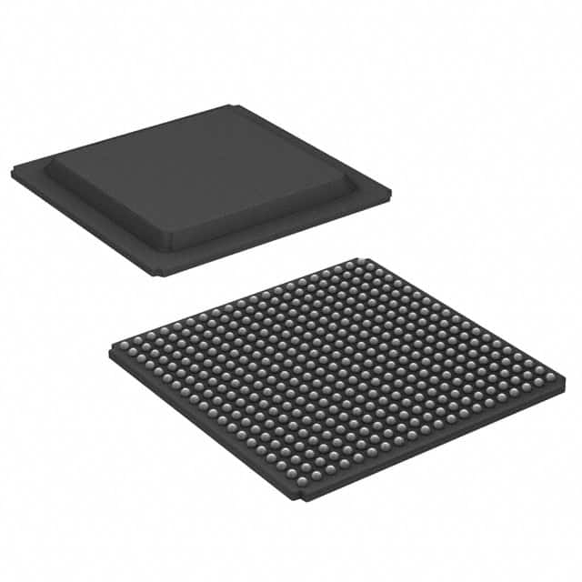
- Robust packaging: The device is packaged in a FG400C package, which provides protection and facilitates easy integration into electronic systems.
Packaging/Quantity
The XC3S400A-4FG400C is available in a compact FG400C package. It is typically sold individually or in small quantities.
Specifications
- Logic Cells: 400,000
- Flip-Flops: 200,000
- Block RAM: 864 Kb
- DSP Slices: 120
- Maximum Frequency: 400 MHz
- I/O Pins: 400
- Operating Voltage: 1.2V
- Package: FG400C
Pin Configuration
The XC3S400A-4FG400C has a detailed pin configuration, which can be found in the product datasheet provided by the manufacturer.
Functional Features
- High-speed processing: The XC3S400A-4FG400C offers fast data processing capabilities, enabling real-time applications.
- Reconfigurability: The FPGA can be reprogrammed multiple times, allowing for flexibility in design modifications.
- Embedded memory: The device includes block RAM, which can be used to store data during operation.
- I/O capabilities: With 400 I/O pins, the XC3S400A-4FG400C provides extensive connectivity options.
Advantages and Disadvantages
Advantages
- High performance and processing speed
- Low power consumption
- Versatility and customization options
- Compact packaging for easy integration
Disadvantages
- Limited logic capacity compared to higher-end FPGAs
- Higher cost compared to other programmable logic devices
Working Principles
The XC3S400A-4FG400C operates based on the principles of digital logic. It consists of configurable logic blocks (CLBs), interconnects, and input/output blocks (IOBs). The CLBs contain look-up tables (LUTs) that can be programmed to implement desired logic functions. The interconnects provide routing paths between different components, enabling data flow. The IOBs facilitate communication between the FPGA and external devices.
Detailed Application Field Plans
The XC3S400A-4FG400C is suitable for a wide range of applications, including: 1. Communications systems: The FPGA can be used in wireless communication devices, routers, and network switches. 2. Industrial automation: It can be employed in control systems, robotics, and process automation. 3. Medical equipment: The XC3S400A-4FG400C can be utilized in medical imaging devices, patient monitoring systems, and diagnostic equipment. 4. Aerospace and defense: It finds applications in radar systems, avionics, and military communication systems. 5. Automotive electronics: The FPGA can be integrated into automotive control units, infotainment systems, and driver assistance systems.
Detailed and Complete Alternative Models
- XC3S200A-4FG400C: A lower-capacity version of the XC3S400A-4FG400C, suitable for less complex designs.
- XC3S1000-4FG400C: A higher-capacity FPGA with increased logic cells and I/O pins, suitable for more demanding applications.
- XC3S50A-4FG400C: A lower-cost option with reduced logic capacity, ideal for cost-sensitive projects.
These alternative models provide a range of options to suit different design requirements.
In conclusion, the XC3S400A-4FG400C is a high-performance FPGA that offers versatility, low power consumption, and robust packaging. Its reconfigurability and extensive I/O capabilities make it suitable for various applications in industries such as communications, industrial automation, medical equipment, aerospace, and automotive electronics. While it has certain limitations in terms of logic capacity and cost, there are alternative models available to cater to different project needs.
Sebutkan 10 pertanyaan dan jawaban umum terkait penerapan XC3S400A-4FG400C dalam solusi teknis
Sure! Here are 10 common questions and answers related to the application of XC3S400A-4FG400C in technical solutions:
Q: What is XC3S400A-4FG400C? A: XC3S400A-4FG400C is a field-programmable gate array (FPGA) from Xilinx, which offers high-performance digital logic capabilities for various technical applications.
Q: What are the key features of XC3S400A-4FG400C? A: Some key features include 400,000 system gates, 400 MHz performance, 4-input look-up tables, 36Kbits of block RAM, and 16 DSP slices.
Q: What are the typical applications of XC3S400A-4FG400C? A: XC3S400A-4FG400C can be used in a wide range of applications such as telecommunications, industrial automation, automotive electronics, medical devices, and aerospace systems.
Q: How can I program XC3S400A-4FG400C? A: XC3S400A-4FG400C can be programmed using Xilinx's Vivado Design Suite or ISE Design Suite software tools, which allow you to write and compile your design code and then program it onto the FPGA.
Q: What is the power supply requirement for XC3S400A-4FG400C? A: The recommended power supply voltage for XC3S400A-4FG400C is 1.14V to 1.26V, with a maximum current consumption of 500mA.
Q: Can XC3S400A-4FG400C interface with other components or devices? A: Yes, XC3S400A-4FG400C supports various communication interfaces such as SPI, I2C, UART, and Ethernet, allowing it to interface with other components or devices in your system.
Q: What is the maximum operating temperature for XC3S400A-4FG400C? A: The maximum junction temperature for XC3S400A-4FG400C is 100°C, so it should be operated within this temperature range to ensure reliable performance.
Q: Can XC3S400A-4FG400C be reprogrammed multiple times? A: Yes, XC3S400A-4FG400C is a reprogrammable FPGA, which means you can program it multiple times to implement different designs or make changes to your existing design.
Q: Are there any development boards available for XC3S400A-4FG400C? A: Yes, Xilinx provides development boards like the Spartan-3A Evaluation Kit, which includes XC3S400A-4FG400C and allows you to prototype and test your designs.
Q: Where can I find more technical documentation and support for XC3S400A-4FG400C? A: You can find detailed technical documentation, application notes, and support resources on Xilinx's official website or by contacting their customer support team.