

Lihat spesifikasi untuk detail produk.
XC3S400-4FGG456I
Product Overview
Category
The XC3S400-4FGG456I belongs to the category of Field Programmable Gate Arrays (FPGAs).
Use
FPGAs are integrated circuits that can be programmed and reprogrammed to perform various digital functions. The XC3S400-4FGG456I is specifically designed for high-performance applications that require complex logic functions.
Characteristics
- High flexibility: FPGAs can be reconfigured to implement different functionalities, making them suitable for prototyping and development.
- Parallel processing: FPGAs can perform multiple operations simultaneously, enabling faster data processing.
- Customizability: Users can design their own digital circuits and algorithms to be implemented on the FPGA.
- Scalability: FPGAs can be easily scaled up or down depending on the complexity of the application.
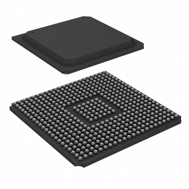
Package
The XC3S400-4FGG456I comes in a FG456 package, which refers to a fine-pitch ball grid array with 456 pins.
Essence
The essence of the XC3S400-4FGG456I lies in its ability to provide a highly configurable and programmable platform for implementing complex digital logic functions.
Packaging/Quantity
The XC3S400-4FGG456I is typically packaged individually and is available in various quantities depending on the manufacturer's specifications.
Specifications
- Logic Cells: 400
- Maximum Frequency: 500 MHz
- Number of I/O Pins: 456
- Operating Voltage: 1.2V
- Operating Temperature Range: -40°C to 100°C
- Configuration Memory: 4Mbit
- Embedded Block RAM: 960Kbit
- DSP Slices: 32
Detailed Pin Configuration
The XC3S400-4FGG456I has a total of 456 pins, each serving a specific purpose. The pin configuration includes input/output pins, power supply pins, clock pins, and configuration pins. For a detailed pinout diagram, please refer to the manufacturer's datasheet.
Functional Features
- High-speed data processing: The XC3S400-4FGG456I can operate at frequencies up to 500 MHz, enabling rapid data processing.
- Configurability: Users can program the FPGA to implement custom logic functions, allowing for versatile applications.
- Embedded memory: The device includes embedded block RAM, providing additional storage for data-intensive applications.
- DSP capabilities: With 32 dedicated DSP slices, the XC3S400-4FGG456I can efficiently perform digital signal processing tasks.
Advantages and Disadvantages
Advantages
- Flexibility: FPGAs offer high flexibility, allowing for quick prototyping and development of complex digital systems.
- Parallel processing: The ability to perform multiple operations simultaneously results in faster data processing.
- Customizability: Users can design their own circuits and algorithms, tailoring the FPGA to specific application requirements.
Disadvantages
- Complexity: Programming an FPGA requires specialized knowledge and expertise.
- Power consumption: FPGAs tend to consume more power compared to other integrated circuits.
- Cost: FPGAs can be relatively expensive compared to other programmable logic devices.
Working Principles
FPGAs consist of an array of configurable logic blocks (CLBs) interconnected through programmable interconnects. The XC3S400-4FGG456I uses look-up tables (LUTs) within the CLBs to implement desired logic functions. These LUTs can be programmed using a hardware description language (HDL) or a graphical programming environment. Once programmed, the FPGA can execute the desired logic functions by routing signals through the interconnects.
Detailed Application Field Plans
The XC3S400-4FGG456I finds applications in various fields, including:
- Communications: The FPGA can be used for implementing high-speed data communication protocols and signal processing algorithms.
- Industrial Automation: It can be employed in control systems, robotics, and machine vision applications.
- Aerospace and Defense: FPGAs are utilized in radar systems, avionics, and secure communications.
- Medical Devices: The XC3S400-4FGG456I can be integrated into medical imaging equipment and diagnostic devices.
- Automotive: FPGAs find applications in advanced driver-assistance systems (ADAS) and infotainment systems.
Detailed and Complete Alternative Models
- XC3S200-4FTG256C
- XC3S1000-4FG320C
- XC3S500E-4PQ208I
- XC3S700A-4FGG484I
- XC3S50A-4VQG100C
These alternative models offer varying capacities, pin configurations, and package options to suit different application requirements.
*
Sebutkan 10 pertanyaan dan jawaban umum terkait penerapan XC3S400-4FGG456I dalam solusi teknis
Sure! Here are 10 common questions and answers related to the application of XC3S400-4FGG456I in technical solutions:
Q: What is XC3S400-4FGG456I? A: XC3S400-4FGG456I is a specific model of Field-Programmable Gate Array (FPGA) manufactured by Xilinx.
Q: What are the key features of XC3S400-4FGG456I? A: Some key features include 400,000 system gates, 456-pin Fine-Pitch Ball Grid Array (FBGA) package, and support for various I/O standards.
Q: What are the typical applications of XC3S400-4FGG456I? A: XC3S400-4FGG456I is commonly used in applications such as digital signal processing, embedded systems, telecommunications, and industrial automation.
Q: How can I program XC3S400-4FGG456I? A: XC3S400-4FGG456I can be programmed using Xilinx's Vivado Design Suite or ISE Design Suite software tools.
Q: What programming languages can be used with XC3S400-4FGG456I? A: XC3S400-4FGG456I can be programmed using Hardware Description Languages (HDLs) such as VHDL or Verilog.
Q: Can XC3S400-4FGG456I be reprogrammed after initial programming? A: Yes, XC3S400-4FGG456I is a reprogrammable FPGA, allowing for multiple programming cycles.
Q: What is the power supply requirement for XC3S400-4FGG456I? A: XC3S400-4FGG456I typically operates at a voltage range of 1.14V to 1.26V.
Q: Does XC3S400-4FGG456I support external memory interfaces? A: Yes, XC3S400-4FGG456I supports various external memory interfaces such as DDR, DDR2, and SDRAM.
Q: Can XC3S400-4FGG456I interface with other devices or microcontrollers? A: Yes, XC3S400-4FGG456I can interface with other devices using standard communication protocols like SPI, I2C, UART, or Ethernet.
Q: Are there any development boards available for XC3S400-4FGG456I? A: Yes, Xilinx provides development boards like the Spartan-3E Starter Kit that are compatible with XC3S400-4FGG456I for prototyping and evaluation purposes.
Please note that these answers are general and may vary depending on specific requirements and use cases.