

Lihat spesifikasi untuk detail produk.
XC3S1600E-4FGG400I
Product Overview
Category
The XC3S1600E-4FGG400I belongs to the category of Field-Programmable Gate Arrays (FPGAs).
Use
FPGAs are integrated circuits that can be programmed and reprogrammed to perform various digital functions. The XC3S1600E-4FGG400I is specifically designed for high-performance applications that require complex logic functions.
Characteristics
- High capacity: The XC3S1600E-4FGG400I has a large number of configurable logic blocks, allowing for the implementation of complex designs.
- Flexibility: FPGAs offer the advantage of being reprogrammable, enabling designers to modify the functionality of the device without changing the hardware.
- Fast processing: With advanced architecture and optimized routing, the XC3S1600E-4FGG400I provides fast processing speeds.
- Low power consumption: This FPGA is designed to minimize power consumption, making it suitable for battery-powered devices.
- High reliability: The XC3S1600E-4FGG400I is built with robust materials and undergoes rigorous testing to ensure reliable operation.
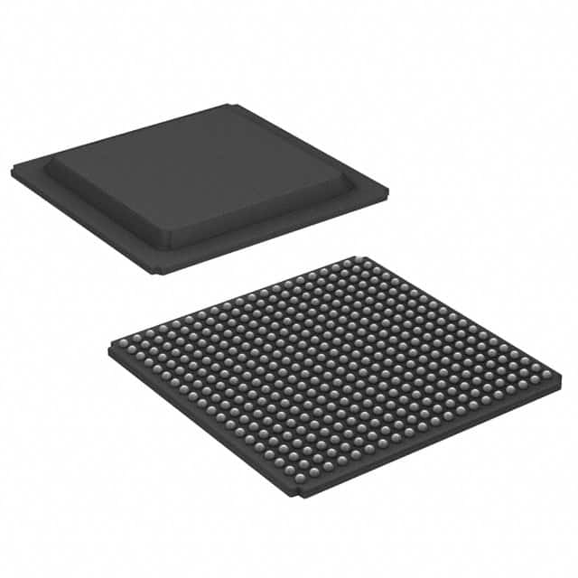
Package
The XC3S1600E-4FGG400I comes in a 400-pin Fine-Pitch Ball Grid Array (FBGA) package.
Essence
The essence of the XC3S1600E-4FGG400I lies in its ability to provide a highly flexible and customizable solution for digital circuit design.
Packaging/Quantity
The XC3S1600E-4FGG400I is typically sold individually or in reels containing multiple units, depending on the supplier. The exact packaging and quantity may vary.
Specifications
- Logic Cells: 1,600
- Maximum Frequency: 500 MHz
- Number of I/Os: 400
- Operating Voltage: 1.2V
- Operating Temperature Range: -40°C to 100°C
- Configuration Memory: 4Mbit
Detailed Pin Configuration
The XC3S1600E-4FGG400I has a total of 400 pins, each serving a specific purpose in the circuit design. A detailed pin configuration diagram can be found in the product datasheet.
Functional Features
- Configurable Logic Blocks (CLBs): The XC3S1600E-4FGG400I contains a large number of CLBs that can be programmed to implement various logic functions.
- Block RAM: This FPGA includes dedicated memory blocks that can be used for data storage and retrieval.
- Digital Clock Manager (DCM): The DCM module allows for precise clock generation and distribution within the FPGA.
- I/O Interfaces: The XC3S1600E-4FGG400I supports various I/O standards, enabling seamless integration with external devices.
- Built-in DSP Blocks: These blocks provide hardware acceleration for digital signal processing tasks.
Advantages and Disadvantages
Advantages
- Flexibility: FPGAs offer the advantage of being highly customizable and reprogrammable, allowing for rapid prototyping and design iterations.
- High Performance: The XC3S1600E-4FGG400I provides fast processing speeds and can handle complex logic functions.
- Low Power Consumption: This FPGA is designed to minimize power consumption, making it suitable for energy-efficient applications.
- Reliability: Xilinx, the manufacturer of XC3S1600E-4FGG400I, is known for producing high-quality and reliable products.
Disadvantages
- Complexity: Working with FPGAs requires specialized knowledge and expertise in digital circuit design.
- Cost: FPGAs can be more expensive compared to other integrated circuits due to their advanced features and flexibility.
Working Principles
FPGAs like the XC3S1600E-4FGG400I consist of an array of configurable logic blocks interconnected through programmable routing resources. The device can be programmed using a Hardware Description Language (HDL) to define the desired functionality. During operation, the FPGA executes the programmed logic functions by routing signals through the configured interconnections.
Detailed Application Field Plans
The XC3S1600E-4FGG400I is suitable for a wide range of applications, including: - Digital signal processing - High-speed data communication - Embedded systems - Robotics - Aerospace and defense systems - Industrial automation
Detailed and Complete Alternative Models
- XC3S200E-4FGG320I: A lower-capacity FPGA from the same family, offering similar features but with fewer logic cells.
- XC3S400E-4FGG320I: A higher-capacity FPGA from the same family, providing increased logic cell count for more complex designs.
- XC3S1000E-4FGG320I: An intermediate
Sebutkan 10 pertanyaan dan jawaban umum terkait penerapan XC3S1600E-4FGG400I dalam solusi teknis
Sure! Here are 10 common questions and answers related to the application of XC3S1600E-4FGG400I in technical solutions:
Q: What is XC3S1600E-4FGG400I? A: XC3S1600E-4FGG400I is a field-programmable gate array (FPGA) from Xilinx, which offers high-performance digital logic capabilities.
Q: What are the key features of XC3S1600E-4FGG400I? A: Some key features include 1.6 million system gates, 1,536 logic cells, 36Kbits of block RAM, 4 digital clock managers, and support for various I/O standards.
Q: What are the typical applications of XC3S1600E-4FGG400I? A: XC3S1600E-4FGG400I is commonly used in applications such as telecommunications, industrial automation, medical devices, aerospace, and defense systems.
Q: How can XC3S1600E-4FGG400I be programmed? A: XC3S1600E-4FGG400I can be programmed using Xilinx's Vivado Design Suite or ISE Design Suite software tools.
Q: What is the maximum operating frequency of XC3S1600E-4FGG400I? A: The maximum operating frequency of XC3S1600E-4FGG400I depends on the specific design and implementation, but it can typically reach frequencies of several hundred megahertz.
Q: Can XC3S1600E-4FGG400I interface with other components or devices? A: Yes, XC3S1600E-4FGG400I supports various I/O standards, including LVCMOS, LVTTL, LVDS, and differential signaling, allowing it to interface with a wide range of components and devices.
Q: What are the power requirements for XC3S1600E-4FGG400I? A: XC3S1600E-4FGG400I typically operates at a voltage of 1.2V, but it also requires additional voltages for I/O banks and configuration.
Q: Can XC3S1600E-4FGG400I be used in safety-critical applications? A: Yes, XC3S1600E-4FGG400I can be used in safety-critical applications, provided that proper design techniques and redundancy measures are implemented to ensure reliability.
Q: Are there any development boards or evaluation kits available for XC3S1600E-4FGG400I? A: Yes, Xilinx offers development boards and evaluation kits specifically designed for XC3S1600E-4FGG400I, which provide a convenient platform for prototyping and testing.
Q: Where can I find more information about XC3S1600E-4FGG400I? A: You can find more detailed information about XC3S1600E-4FGG400I in the official documentation provided by Xilinx, such as datasheets, user guides, and application notes.