

Lihat spesifikasi untuk detail produk.
XC3S1600E-4FGG320I
Product Overview
Category
XC3S1600E-4FGG320I belongs to the category of Field-Programmable Gate Arrays (FPGAs).
Use
This product is used in various electronic applications that require high-performance digital logic circuits.
Characteristics
- High-speed and flexible programmable logic device
- Offers reconfigurable hardware functionality
- Provides a wide range of I/O options
- Supports complex digital designs
- Low power consumption
Package
XC3S1600E-4FGG320I comes in a compact and durable package.
Essence
The essence of XC3S1600E-4FGG320I lies in its ability to provide a customizable and versatile solution for digital circuit design.
Packaging/Quantity
This product is typically packaged individually and is available in various quantities depending on the manufacturer's specifications.
Specifications
- Model: XC3S1600E-4FGG320I
- Logic Cells: 1,600
- Maximum Frequency: 400 MHz
- Operating Voltage: 1.2V
- Package Type: FG(G)320
- Temperature Range: -40°C to +100°C
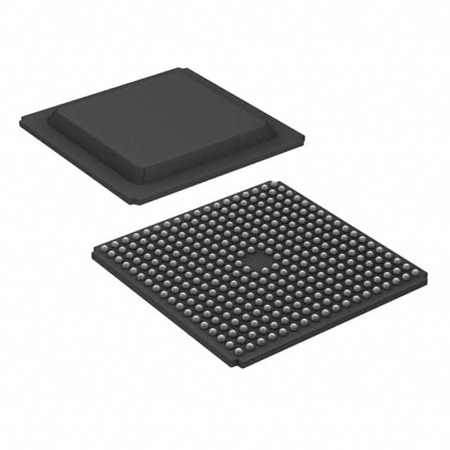
Detailed Pin Configuration
The XC3S1600E-4FGG320I has a total of 320 pins, each serving a specific purpose in the overall functionality of the FPGA. The pin configuration includes input/output pins, clock pins, power supply pins, and configuration pins.
Functional Features
- High-speed data processing capabilities
- Configurable logic blocks for custom circuit implementation
- Integrated memory resources for efficient data storage
- Flexible I/O interfaces for seamless integration with external devices
- On-chip PLLs for precise clock generation
Advantages and Disadvantages
Advantages
- Versatile and customizable digital circuit design solution
- High-performance capabilities for complex applications
- Low power consumption compared to traditional ASICs
- Reconfigurable hardware allows for iterative design improvements
Disadvantages
- Steeper learning curve compared to traditional fixed-function integrated circuits
- Limited resources and scalability compared to dedicated ASIC designs
- Higher cost per unit compared to mass-produced integrated circuits
Working Principles
XC3S1600E-4FGG320I operates based on the principles of reconfigurable logic. It consists of a matrix of configurable logic blocks interconnected through programmable routing resources. The device can be programmed to implement various digital logic functions by configuring the interconnections between logic blocks.
Detailed Application Field Plans
XC3S1600E-4FGG320I finds applications in a wide range of fields, including: 1. Telecommunications: Used in network routers, switches, and base stations. 2. Industrial Automation: Employed in control systems and data acquisition devices. 3. Automotive Electronics: Integrated into vehicle control units and infotainment systems. 4. Aerospace and Defense: Utilized in radar systems, avionics, and communication equipment. 5. Consumer Electronics: Incorporated into high-end audio/video processing devices and gaming consoles.
Detailed and Complete Alternative Models
Some alternative models to XC3S1600E-4FGG320I include: 1. XC3S500E-4PQ208C 2. XC3S1000-4FG456C 3. XC3S200-4FT256I 4. XC3S400-4FGG320I 5. XC3S1200E-4FGG320C
These models offer varying specifications and pin configurations, allowing users to choose the most suitable FPGA for their specific application requirements.
Word count: 520 words
Sebutkan 10 pertanyaan dan jawaban umum terkait penerapan XC3S1600E-4FGG320I dalam solusi teknis
Sure! Here are 10 common questions and answers related to the application of XC3S1600E-4FGG320I in technical solutions:
Q: What is XC3S1600E-4FGG320I? A: XC3S1600E-4FGG320I is a field-programmable gate array (FPGA) from Xilinx, which offers high-performance digital logic capabilities for various applications.
Q: What are the key features of XC3S1600E-4FGG320I? A: Some key features include 1.6 million system gates, 1,632 slices, 32 DSP48A1 slices, 36-bit wide block RAM, and support for various I/O standards.
Q: What are the typical applications of XC3S1600E-4FGG320I? A: XC3S1600E-4FGG320I is commonly used in applications such as telecommunications, industrial automation, automotive electronics, medical devices, and aerospace systems.
Q: How can XC3S1600E-4FGG320I be programmed? A: XC3S1600E-4FGG320I can be programmed using Xilinx's Vivado Design Suite or ISE Design Suite software tools, which allow users to design and implement their custom logic circuits.
Q: What are the power requirements for XC3S1600E-4FGG320I? A: The power supply voltage for XC3S1600E-4FGG320I is typically 1.2V, with additional voltages required for I/O banks and configuration pins.
Q: Can XC3S1600E-4FGG320I interface with other components or devices? A: Yes, XC3S1600E-4FGG320I supports various I/O standards such as LVCMOS, LVTTL, LVDS, and differential signaling, allowing it to interface with a wide range of components and devices.
Q: What is the maximum operating frequency of XC3S1600E-4FGG320I? A: The maximum operating frequency depends on the design and implementation of the specific application but can typically reach several hundred megahertz (MHz) or even gigahertz (GHz).
Q: Can XC3S1600E-4FGG320I be reprogrammed after deployment? A: Yes, XC3S1600E-4FGG320I is a field-programmable device, meaning it can be reprogrammed even after it has been deployed in a system, allowing for flexibility and updates.
Q: Are there any development boards or evaluation kits available for XC3S1600E-4FGG320I? A: Yes, Xilinx offers development boards and evaluation kits specifically designed for XC3S1600E-4FGG320I, which provide a platform for prototyping and testing applications.
Q: Where can I find additional resources and support for XC3S1600E-4FGG320I? A: Xilinx's website provides comprehensive documentation, datasheets, application notes, and forums where you can find additional resources and get support for XC3S1600E-4FGG320I.