

Lihat spesifikasi untuk detail produk.
XC3030A-7PC84C
Product Overview
Category
XC3030A-7PC84C belongs to the category of programmable logic devices (PLDs).
Use
This product is commonly used in digital circuit design and implementation. It provides a flexible and customizable solution for various applications.
Characteristics
- Programmable: The XC3030A-7PC84C can be programmed to perform specific functions based on the user's requirements.
- High-density: It offers a high number of logic gates, allowing for complex designs.
- Low power consumption: The device is designed to operate efficiently with minimal power usage.
- Fast operation: The XC3030A-7PC84C has a high-speed performance, enabling quick execution of logic operations.
Package
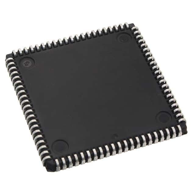
The XC3030A-7PC84C comes in a 84-pin plastic leaded chip carrier (PC84C) package.
Essence
The essence of XC3030A-7PC84C lies in its ability to provide reconfigurable logic functionality, allowing designers to implement custom digital circuits without the need for dedicated hardware.
Packaging/Quantity
The XC3030A-7PC84C is typically packaged individually and is available in various quantities depending on the manufacturer or distributor.
Specifications
- Logic Cells: 300
- Maximum User I/Os: 68
- Operating Voltage: 3.3V
- Speed Grade: -7
- Package Type: PC84C
- Temperature Range: -40°C to +85°C
Detailed Pin Configuration
The XC3030A-7PC84C has a total of 84 pins. The pin configuration is as follows:
- VCCIO
- GND
- IO1
- IO2
- IO3
- IO4
- IO5
- IO6
- IO7
- IO8
- IO9
- IO10
- IO11
- IO12
- IO13
- IO14
- IO15
- IO16
- IO17
- IO18
- IO19
- IO20
- IO21
- IO22
- IO23
- IO24
- IO25
- IO26
- IO27
- IO28
- IO29
- IO30
- IO31
- IO32
- IO33
- IO34
- IO35
- IO36
- IO37
- IO38
- IO39
- IO40
- IO41
- IO42
- IO43
- IO44
- IO45
- IO46
- IO47
- IO48
- IO49
- IO50
- IO51
- IO52
- IO53
- IO54
- IO55
- IO56
- IO57
- IO58
- IO59
- IO60
- IO61
- IO62
- IO63
- IO64
- IO65
- IO66
- IO67
- IO68
- GND
- VCCIO
- TCK
- TMS
- TDI
- TDO
- GND
- VCCIO
- GND
- VCCIO
- GND
- VCCIO
- GND
- VCCIO
Functional Features
- Reconfigurable Logic: The XC3030A-7PC84C allows users to modify the logic functions according to their specific requirements.
- High-Speed Operation: It offers fast execution of logic operations, enabling efficient processing of digital signals.
- Flexible I/O Configuration: The device provides a wide range of input/output options, allowing for versatile connectivity with external components.
- On-Chip Memory: The XC3030A-7PC84C includes embedded memory elements that can be used for storing data or configuration settings.
Advantages and Disadvantages
Advantages
- Flexibility: The reconfigurable nature of the XC3030A-7PC84C enables designers to adapt their circuits as needed.
- Cost-Effective: By eliminating the need for dedicated hardware, this PLD reduces overall system costs.
- Time-Saving: The programmable nature of the device allows for faster prototyping and development cycles.
Disadvantages
- Complexity: Designing and programming the XC3030A-7PC84C requires expertise in digital circuit design and programming languages.
Sebutkan 10 pertanyaan dan jawaban umum terkait penerapan XC3030A-7PC84C dalam solusi teknis
Sure! Here are 10 common questions and answers related to the application of XC3030A-7PC84C in technical solutions:
Q: What is XC3030A-7PC84C? A: XC3030A-7PC84C is a specific model of field-programmable gate array (FPGA) manufactured by Xilinx.
Q: What are the key features of XC3030A-7PC84C? A: Some key features of XC3030A-7PC84C include 3000 usable gates, 84-pin plastic leaded chip carrier (PLCC) package, and 5V operation.
Q: How can XC3030A-7PC84C be used in technical solutions? A: XC3030A-7PC84C can be used for various applications such as digital signal processing, data communication, control systems, and more.
Q: What programming languages are supported for XC3030A-7PC84C? A: XC3030A-7PC84C can be programmed using hardware description languages (HDLs) like VHDL or Verilog.
Q: Can XC3030A-7PC84C be reprogrammed after initial configuration? A: No, XC3030A-7PC84C is not a reprogrammable FPGA. Once it is configured, the design remains fixed.
Q: What is the power supply requirement for XC3030A-7PC84C? A: XC3030A-7PC84C operates at 5V DC power supply.
Q: Are there any development tools available for programming XC3030A-7PC84C? A: Yes, Xilinx provides development tools like Xilinx ISE Design Suite or Vivado Design Suite for programming and configuring XC3030A-7PC84C.
Q: Can XC3030A-7PC84C be used in high-speed applications? A: Yes, XC3030A-7PC84C can be used in high-speed applications as it supports clock frequencies up to 50 MHz.
Q: What is the maximum number of inputs and outputs supported by XC3030A-7PC84C? A: XC3030A-7PC84C supports up to 68 inputs and 32 outputs.
Q: Is XC3030A-7PC84C still widely available in the market? A: No, XC3030A-7PC84C is an older FPGA model and may not be readily available. It has been superseded by newer models.