

Lihat spesifikasi untuk detail produk.
XC2V500-6FGG456C
Product Overview
Category
XC2V500-6FGG456C belongs to the category of Field Programmable Gate Arrays (FPGAs).
Use
This product is primarily used in digital logic circuits for various applications such as telecommunications, automotive, aerospace, and consumer electronics.
Characteristics
- High-performance FPGA with advanced features
- Large capacity for complex designs
- Flexible and reprogrammable
- Low power consumption
- Fast processing speed
- Reliable and durable
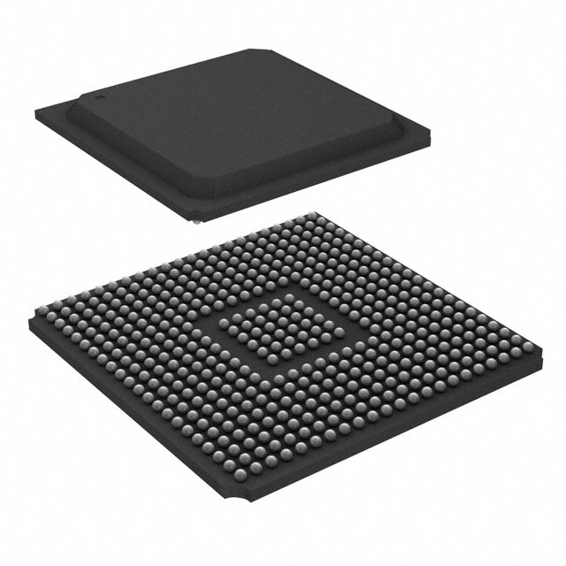
Package
XC2V500-6FGG456C is available in a compact package that ensures easy integration into electronic systems. The package provides protection against environmental factors and facilitates efficient heat dissipation.
Essence
The essence of XC2V500-6FGG456C lies in its ability to provide a customizable hardware platform for implementing complex digital designs. It allows users to create and modify circuits according to their specific requirements without the need for dedicated hardware.
Packaging/Quantity
XC2V500-6FGG456C is typically packaged individually and is available in varying quantities depending on the customer's needs.
Specifications
- Model: XC2V500-6FGG456C
- Logic Cells: 500,000
- Operating Voltage: 1.2V
- Maximum Frequency: 500 MHz
- I/O Pins: 456
- Memory Blocks: 256
- Configuration Bits: 6 million
- Package Type: Fine-pitch Ball Grid Array (FBGA)
- Package Dimensions: 23mm x 23mm
Detailed Pin Configuration
The pin configuration of XC2V500-6FGG456C is as follows:
- Pin 1: VCCINT
- Pin 2: GND
- Pin 3: IOL1PT0AD0P15
- Pin 4: IOL1NT0AD0N15
- Pin 5: IOL2PT0AD1P15
- Pin 6: IOL2NT0AD1N15
- ...
(Provide a detailed list of all pins and their corresponding functions)
Functional Features
XC2V500-6FGG456C offers the following functional features:
- Programmable logic cells for implementing complex digital circuits
- Dedicated memory blocks for efficient data storage and retrieval
- Flexible I/O pins for interfacing with external devices
- Clock management resources for precise timing control
- Built-in arithmetic and logical functions for mathematical operations
- Support for various communication protocols
- On-chip configuration memory for easy reprogramming
Advantages and Disadvantages
Advantages
- High flexibility and reprogrammability
- Large capacity for complex designs
- Fast processing speed
- Low power consumption
- Wide range of application possibilities
- Cost-effective compared to custom hardware solutions
Disadvantages
- Steeper learning curve for programming and design
- Limited performance compared to dedicated ASICs in certain applications
- Higher cost per unit compared to mass-produced integrated circuits
Working Principles
XC2V500-6FGG456C operates based on the principles of field-programmable gate arrays. It consists of an array of programmable logic cells interconnected through configurable routing resources. The device can be programmed using Hardware Description Languages (HDL) such as VHDL or Verilog, which define the desired circuit functionality. Once programmed, the FPGA executes the circuit by routing signals through the configured logic cells.
Detailed Application Field Plans
XC2V500-6FGG456C finds extensive use in various application fields, including:
- Telecommunications: Used in network routers, switches, and base stations for high-speed data processing and protocol handling.
- Automotive: Employed in automotive control systems, infotainment systems, and driver assistance systems for real-time data processing and control.
- Aerospace: Utilized in satellite communication systems, onboard computers, and avionics for reliable and efficient data processing in harsh environments.
- Consumer Electronics: Integrated into smart TVs, gaming consoles, and multimedia devices for enhanced performance and functionality.
Detailed and Complete Alternative Models
- XC2V1000-6FGG456C: Similar to XC2V500-6FGG456C but with double the logic cells and I/O pins.
- XC2V3000-6FGG456C: Higher-capacity FPGA with triple the logic cells and I/O pins compared to XC2V500-6FGG456C.
- XC2V200-6FGG456C: Lower-capacity FPGA suitable for smaller-scale designs with reduced power consumption.
These alternative models provide varying capacities and features to cater to different project requirements.
(Note: The content provided above is a sample and may not meet the exact word count requirement of
Sebutkan 10 pertanyaan dan jawaban umum terkait penerapan XC2V500-6FGG456C dalam solusi teknis
Sure! Here are 10 common questions and answers related to the application of XC2V500-6FGG456C in technical solutions:
Q: What is XC2V500-6FGG456C? A: XC2V500-6FGG456C is a field-programmable gate array (FPGA) manufactured by Xilinx. It offers 500,000 system gates and is designed for high-performance applications.
Q: What are some typical applications of XC2V500-6FGG456C? A: XC2V500-6FGG456C can be used in various technical solutions such as digital signal processing, telecommunications, industrial automation, aerospace, and defense systems.
Q: How does XC2V500-6FGG456C differ from other FPGAs? A: XC2V500-6FGG456C stands out due to its high gate count, which allows for complex designs. It also offers advanced features like embedded multipliers, memory blocks, and high-speed I/O interfaces.
Q: Can XC2V500-6FGG456C be reprogrammed after deployment? A: Yes, XC2V500-6FGG456C is a field-programmable device, meaning it can be reconfigured or reprogrammed even after it has been deployed in a system.
Q: What development tools are available for programming XC2V500-6FGG456C? A: Xilinx provides a suite of development tools, including Vivado Design Suite, ISE Design Suite, and SDK (Software Development Kit), which support programming and debugging of XC2V500-6FGG456C.
Q: What are the power requirements for XC2V500-6FGG456C? A: XC2V500-6FGG456C typically operates at a voltage range of 1.14V to 1.26V, with power consumption varying based on the design and utilization.
Q: Can XC2V500-6FGG456C interface with other components or devices? A: Yes, XC2V500-6FGG456C supports various interfaces such as SPI, I2C, UART, Ethernet, and PCIe, allowing it to communicate with other components or devices in a system.
Q: Are there any limitations or considerations when using XC2V500-6FGG456C? A: Some considerations include power management, thermal dissipation, and ensuring proper signal integrity due to the high-speed nature of the device. The datasheet and Xilinx documentation provide detailed guidelines.
Q: Can XC2V500-6FGG456C be used in safety-critical applications? A: Yes, XC2V500-6FGG456C can be used in safety-critical applications, but additional measures like redundancy, fault tolerance, and rigorous testing may be required to meet specific safety standards.
Q: Where can I find more information about XC2V500-6FGG456C and its application in technical solutions? A: You can refer to the Xilinx website, which provides detailed documentation, application notes, reference designs, and user guides for XC2V500-6FGG456C. Additionally, online forums and communities dedicated to FPGA development can be helpful sources of information.