

Lihat spesifikasi untuk detail produk.
XC2V1000-5BGG575C
Product Overview
Category
The XC2V1000-5BGG575C belongs to the category of Field Programmable Gate Arrays (FPGAs).
Use
FPGAs are integrated circuits that can be programmed and reprogrammed to perform various digital functions. The XC2V1000-5BGG575C is specifically designed for high-performance applications.
Characteristics
- High-speed processing capabilities
- Configurable logic blocks
- On-chip memory
- Flexible I/O options
- Low power consumption
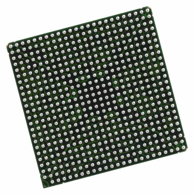
Package
The XC2V1000-5BGG575C comes in a Ball Grid Array (BGA) package, which provides a compact and reliable form factor for mounting on circuit boards.
Essence
The essence of the XC2V1000-5BGG575C lies in its ability to provide customizable digital logic functions, allowing designers to implement complex systems on a single chip.
Packaging/Quantity
The XC2V1000-5BGG575C is typically packaged in reels or trays, with each package containing a specific quantity of chips. The exact quantity may vary depending on the supplier.
Specifications
- Device type: FPGA
- Family: Virtex-II
- Logic cells: 1,000
- Speed grade: -5
- Package type: BGA
- Package size: 575 balls
- Operating temperature range: -40°C to +85°C
- Supply voltage: 3.3V
Detailed Pin Configuration
The XC2V1000-5BGG575C has a total of 575 pins arranged in a specific configuration. Please refer to the datasheet provided by the manufacturer for detailed pin assignments.
Functional Features
- Configurable logic blocks allow for flexible implementation of digital circuits.
- On-chip memory resources enable efficient data storage and retrieval.
- Flexible I/O options provide connectivity to external devices.
- High-speed processing capabilities enable real-time applications.
- Low power consumption ensures energy efficiency.
Advantages and Disadvantages
Advantages
- Versatility: FPGAs can be reprogrammed for different applications, providing flexibility in system design.
- Rapid Prototyping: FPGAs allow for quick development and testing of digital circuits.
- Integration: Multiple functions can be implemented on a single chip, reducing the need for additional components.
- Customizability: FPGAs can be tailored to specific requirements, optimizing performance and functionality.
Disadvantages
- Complexity: Designing complex systems with FPGAs requires expertise in digital circuit design.
- Cost: FPGAs can be more expensive compared to other integrated circuits.
- Power Consumption: While efforts have been made to reduce power consumption, FPGAs still consume more power compared to dedicated ASICs.
Working Principles
FPGAs consist of an array of configurable logic blocks interconnected through programmable routing resources. The XC2V1000-5BGG575C utilizes a combination of look-up tables, flip-flops, and interconnect resources to implement desired digital functions. The configuration of these elements is determined by programming the FPGA using Hardware Description Languages (HDL) or specialized design tools.
Detailed Application Field Plans
The XC2V1000-5BGG575C finds applications in various fields, including:
- Telecommunications: Used in base stations, network routers, and communication infrastructure for high-speed data processing.
- Aerospace and Defense: Employed in radar systems, avionics, and military-grade communication equipment for their high-performance capabilities.
- Industrial Automation: Utilized in control systems, robotics, and machine vision applications for real-time processing and control.
- Medical Devices: Integrated into medical imaging systems, patient monitoring devices, and diagnostic equipment for their processing power and flexibility.
- Automotive: Used in advanced driver assistance systems (ADAS), infotainment systems, and engine control units (ECUs) for enhanced functionality and performance.
Detailed and Complete Alternative Models
- XC2V2000-4FGG676C: A higher-capacity FPGA from the same Virtex-II family, offering 2,000 logic cells and a different package configuration.
- XC7A35T-1CPG236C: An FPGA from the newer Artix-7 family, featuring lower power consumption and improved performance characteristics.
- EP4CE6E22C8N: An FPGA from Altera's Cyclone IV family, providing a cost-effective solution with moderate performance capabilities.
These alternative models offer different specifications and features, catering to diverse application requirements.
Word count: 560 words
Sebutkan 10 pertanyaan dan jawaban umum terkait penerapan XC2V1000-5BGG575C dalam solusi teknis
Sure! Here are 10 common questions and answers related to the application of XC2V1000-5BGG575C in technical solutions:
Q: What is XC2V1000-5BGG575C? A: XC2V1000-5BGG575C is a specific model of Field Programmable Gate Array (FPGA) manufactured by Xilinx.
Q: What are the key features of XC2V1000-5BGG575C? A: Some key features include 1,000,000 system gates, 576 user I/Os, 5ns pin-to-pin delay, and 1.8V core voltage.
Q: What are the typical applications of XC2V1000-5BGG575C? A: XC2V1000-5BGG575C is commonly used in various technical solutions such as digital signal processing, embedded systems, telecommunications, and industrial automation.
Q: How can XC2V1000-5BGG575C be programmed? A: XC2V1000-5BGG575C can be programmed using Xilinx's proprietary software called Vivado or ISE Design Suite.
Q: Can XC2V1000-5BGG575C be reprogrammed after it has been programmed once? A: Yes, XC2V1000-5BGG575C is a reprogrammable FPGA, which means it can be reprogrammed multiple times.
Q: What is the power consumption of XC2V1000-5BGG575C? A: The power consumption of XC2V1000-5BGG575C depends on the specific design and usage scenario. It is typically in the range of a few watts.
Q: Does XC2V1000-5BGG575C support different communication protocols? A: Yes, XC2V1000-5BGG575C supports various communication protocols such as UART, SPI, I2C, Ethernet, and more.
Q: Can XC2V1000-5BGG575C interface with external memory devices? A: Yes, XC2V1000-5BGG575C has dedicated pins for interfacing with external memory devices like DDR SDRAM, SRAM, Flash, etc.
Q: What is the maximum clock frequency that XC2V1000-5BGG575C can operate at? A: The maximum clock frequency of XC2V1000-5BGG575C depends on the specific design and implementation. It can typically operate in the range of tens to hundreds of megahertz.
Q: Are there any development boards or evaluation kits available for XC2V1000-5BGG575C? A: Yes, Xilinx provides development boards and evaluation kits specifically designed for XC2V1000-5BGG575C, which can help in prototyping and testing applications.
Please note that the answers provided here are general and may vary depending on the specific requirements and use cases.