

Lihat spesifikasi untuk detail produk.
XC2S15-5VQ100C
Product Overview
Category
XC2S15-5VQ100C belongs to the category of programmable logic devices (PLDs).
Use
This product is used for digital circuit design and implementation. It provides a flexible and customizable solution for various applications.
Characteristics
- Programmable: The XC2S15-5VQ100C can be programmed to perform specific functions based on user requirements.
- High-speed operation: It offers fast processing capabilities, making it suitable for applications that require quick response times.
- Low power consumption: The device is designed to minimize power usage, making it energy-efficient.
- Versatile: It supports a wide range of applications due to its programmability.
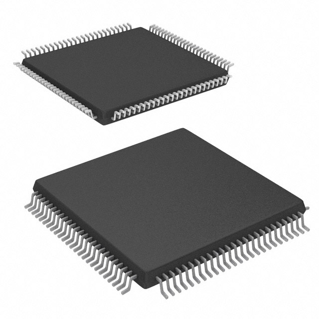
Package
The XC2S15-5VQ100C comes in a VQ100 package, which is a quad flat pack with 100 pins.
Essence
The essence of XC2S15-5VQ100C lies in its ability to provide reconfigurable logic functions, allowing users to implement complex digital circuits efficiently.
Packaging/Quantity
This product is typically packaged in reels or trays, with each containing a specific quantity of XC2S15-5VQ100C devices. The exact quantity may vary depending on the manufacturer's specifications.
Specifications
- Device type: Programmable logic device (PLD)
- Family: XC2S
- Series: Spartan-II
- Number of logic cells: 1,500
- Number of I/O pins: 100
- Operating voltage: 5V
- Speed grade: -5
- Package type: VQ100
Detailed Pin Configuration
The XC2S15-5VQ100C has a total of 100 pins, each serving a specific purpose. The pin configuration is as follows:
(Pin Number) (Pin Name) (Description) 1 VCCINT Power supply for internal circuitry 2-9 IOB0-IOB7 Bidirectional I/O pins 10 GND Ground 11-18 IOB8-IOB15 Bidirectional I/O pins 19 VCCO0 Output power supply for bank 0 20-27 IOB16-IOB23 Bidirectional I/O pins 28 GND Ground 29-36 IOB24-IOB31 Bidirectional I/O pins 37 VCCO1 Output power supply for bank 1 38-45 IOB32-IOB39 Bidirectional I/O pins 46 GND Ground 47-54 IOB40-IOB47 Bidirectional I/O pins 55 VCCO2 Output power supply for bank 2 56-63 IOB48-IOB55 Bidirectional I/O pins 64 GND Ground 65-72 IOB56-IOB63 Bidirectional I/O pins 73 VCCO3 Output power supply for bank 3 74-81 IOB64-IOB71 Bidirectional I/O pins 82 GND Ground 83-90 IOB72-IOB79 Bidirectional I/O pins 91 VCCO_4 Output power supply for bank 4 92-99 IOB80-IOB87 Bidirectional I/O pins 100 GND Ground
Functional Features
The XC2S15-5VQ100C offers the following functional features:
- Configurable logic blocks: These blocks can be programmed to perform various logic functions, such as AND, OR, and XOR.
- Programmable interconnects: The device allows users to establish connections between different logic blocks, enabling the creation of complex digital circuits.
- Input/output buffers: These buffers facilitate communication between the device and external components.
- Clock management: The XC2S15-5VQ100C supports clock signals for synchronous operation.
Advantages and Disadvantages
Advantages
- Flexibility: The programmable nature of XC2S15-5VQ100C allows for customization and adaptability to different applications.
- High-speed operation: The device offers fast processing capabilities, making it suitable for time-critical applications.
- Low power consumption: The XC2S15-5VQ100C is designed to minimize power usage, resulting in energy-efficient operation.
Disadvantages
- Complexity: Programming and configuring the XC2S15-5VQ100C may require specialized knowledge and expertise.
- Limited resources: Compared to larger PLDs, this device has a limited number of logic cells and I/O pins, which may restrict the complexity of designs that can be implemented.
Working Principles
The XC2S15-5VQ100C operates based
Sebutkan 10 pertanyaan dan jawaban umum terkait penerapan XC2S15-5VQ100C dalam solusi teknis
Sure! Here are 10 common questions and answers related to the application of XC2S15-5VQ100C in technical solutions:
Question: What is XC2S15-5VQ100C?
- Answer: XC2S15-5VQ100C is a specific model of Field Programmable Gate Array (FPGA) manufactured by Xilinx.Question: What are the key features of XC2S15-5VQ100C?
- Answer: Some key features of XC2S15-5VQ100C include 15,000 system gates, 192 logic cells, 64 I/O pins, and support for 5V operation.Question: What are the typical applications of XC2S15-5VQ100C?
- Answer: XC2S15-5VQ100C is commonly used in various technical solutions such as industrial control systems, communication equipment, automotive electronics, and medical devices.Question: Can XC2S15-5VQ100C be programmed after it is installed in a system?
- Answer: Yes, XC2S15-5VQ100C is a programmable device that can be reprogrammed even after it is soldered onto a PCB.Question: What programming languages can be used to program XC2S15-5VQ100C?
- Answer: XC2S15-5VQ100C can be programmed using Hardware Description Languages (HDLs) such as VHDL or Verilog.Question: Is XC2S15-5VQ100C suitable for high-speed applications?
- Answer: Yes, XC2S15-5VQ100C supports high-speed operation and can be used in applications that require fast data processing.Question: Can XC2S15-5VQ100C interface with other components or devices?
- Answer: Yes, XC2S15-5VQ100C has multiple I/O pins that can be used to interface with other components or devices in a system.Question: What is the power supply requirement for XC2S15-5VQ100C?
- Answer: XC2S15-5VQ100C operates at 5V and requires a stable power supply within the specified voltage range.Question: Can XC2S15-5VQ100C be used in battery-powered applications?
- Answer: While XC2S15-5VQ100C supports low-power operation, it may not be the most suitable choice for battery-powered applications due to its higher power consumption compared to some other FPGAs.Question: Are there any development tools available for programming XC2S15-5VQ100C?
- Answer: Yes, Xilinx provides development tools such as Vivado Design Suite that can be used to program and configure XC2S15-5VQ100C.
Please note that the answers provided here are general and may vary depending on specific requirements and application scenarios.