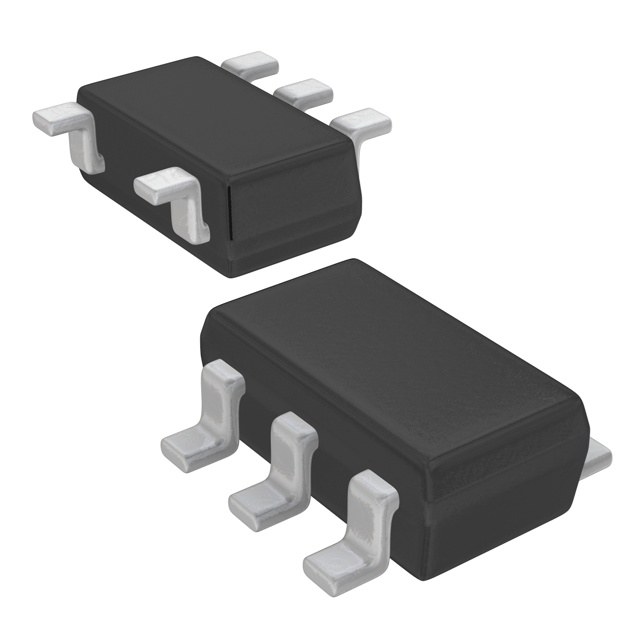
Lihat spesifikasi untuk detail produk.

XC6124D633MR-G
Product Overview
- Category: Integrated Circuit (IC)
- Use: Voltage Regulator
- Characteristics: Low Dropout, Low Quiescent Current, High Accuracy
- Package: SOT-23-5
- Essence: Regulates voltage to ensure stable power supply
- Packaging/Quantity: Tape and Reel, 3000 units per reel
Specifications
- Input Voltage Range: 2.5V - 6.0V
- Output Voltage Range: 1.2V - 5.5V
- Dropout Voltage: 200mV @ 100mA
- Quiescent Current: 30µA
- Output Current: 150mA
- Line Regulation: ±0.05%
- Load Regulation: ±0.1%
- Operating Temperature Range: -40°C to +85°C
Detailed Pin Configuration
The XC6124D633MR-G has a total of five pins arranged as follows:
```
| | --| VOUT GND|-- Pin 1 --| VIN NC |-- Pin 2 --| EN NC |-- Pin 3 --| NC NC |-- Pin 4 --| VIN NC |-- Pin 5 |___________| ```
Functional Features
- Low Dropout: The XC6124D633MR-G can regulate the output voltage even when the input voltage is close to the desired output voltage.
- Low Quiescent Current: It consumes very low current when in standby mode, resulting in increased battery life.
- High Accuracy: The voltage regulator provides precise and stable output voltage, ensuring reliable performance.
Advantages and Disadvantages
Advantages: - Low dropout voltage ensures efficient power conversion. - Low quiescent current prolongs battery life. - High accuracy guarantees stable output voltage.
Disadvantages: - Limited output current of 150mA may not be sufficient for high-power applications. - The SOT-23-5 package may require additional space on the PCB.
Working Principles
The XC6124D633MR-G is a linear voltage regulator that uses a pass transistor to regulate the output voltage. It compares the reference voltage with the feedback voltage and adjusts the pass transistor accordingly to maintain a stable output voltage. The dropout voltage is minimized by using a low resistance pass transistor.
Detailed Application Field Plans
The XC6124D633MR-G is commonly used in various electronic devices, including:
- Mobile Phones: Provides stable power supply for the processor, memory, and other components.
- Portable Audio Players: Regulates voltage for audio amplifiers and digital-to-analog converters.
- Wearable Devices: Ensures reliable power delivery to sensors, displays, and communication modules.
- IoT Devices: Maintains stable voltage for microcontrollers, sensors, and wireless communication modules.
Detailed and Complete Alternative Models
- XC6206P332MR-G: Similar voltage regulator with a lower dropout voltage of 120mV @ 100mA.
- XC6220B332MR-G: Voltage regulator with higher output current capability of 300mA.
- XC6219B332MR-G: Low quiescent current voltage regulator with only 10µA standby current.
These alternative models provide options based on specific requirements such as dropout voltage, output current, and standby current.
In conclusion, the XC6124D633MR-G is a voltage regulator IC that offers low dropout, low quiescent current, and high accuracy. It is commonly used in various electronic devices to ensure stable power supply. While it has limitations in terms of output current and package size, there are alternative models available to suit different application needs.
Sebutkan 10 pertanyaan dan jawaban umum terkait penerapan XC6124D633MR-G dalam solusi teknis
Sure! Here are 10 common questions and answers related to the application of XC6124D633MR-G in technical solutions:
Question: What is XC6124D633MR-G?
Answer: XC6124D633MR-G is a voltage detector IC manufactured by Torex Semiconductor. It is used to monitor the power supply voltage and provide a reset signal when the voltage drops below a certain threshold.Question: What is the operating voltage range of XC6124D633MR-G?
Answer: The operating voltage range of XC6124D633MR-G is from 0.6V to 6.0V.Question: How does XC6124D633MR-G detect the voltage level?
Answer: XC6124D633MR-G uses an internal voltage reference and a comparator to compare the input voltage with a preset threshold voltage.Question: What is the typical threshold voltage of XC6124D633MR-G?
Answer: The typical threshold voltage of XC6124D633MR-G is 3.3V.Question: Can XC6124D633MR-G be used in battery-powered applications?
Answer: Yes, XC6124D633MR-G can be used in battery-powered applications as it has a low quiescent current consumption of typically 1.0µA.Question: Does XC6124D633MR-G have any built-in delay time for the reset signal?
Answer: Yes, XC6124D633MR-G has a built-in delay time of typically 200ms to prevent false resets caused by momentary voltage fluctuations.Question: What is the output configuration of XC6124D633MR-G?
Answer: XC6124D633MR-G has an open-drain output configuration, which requires an external pull-up resistor.Question: Can XC6124D633MR-G be used in automotive applications?
Answer: Yes, XC6124D633MR-G is AEC-Q100 qualified and can be used in automotive applications.Question: What is the temperature range of XC6124D633MR-G?
Answer: The operating temperature range of XC6124D633MR-G is from -40°C to +85°C.Question: Is XC6124D633MR-G available in different package options?
Answer: Yes, XC6124D633MR-G is available in a SOT-25 package, which is a small surface-mount package with 5 pins.
Please note that these answers are based on general information about XC6124D633MR-G and may vary depending on specific application requirements.

