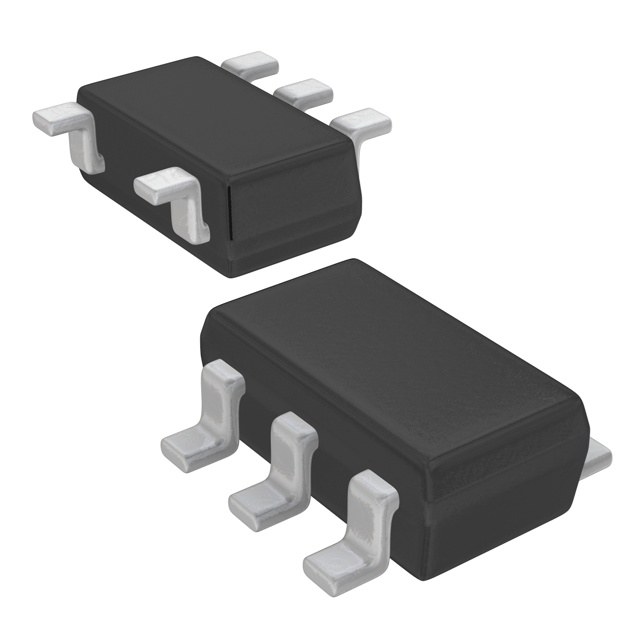
Lihat spesifikasi untuk detail produk.

XC6123D633MR-G
Product Overview
Category
XC6123D633MR-G belongs to the category of voltage regulators.
Use
It is commonly used for regulating voltage in electronic circuits.
Characteristics
- Package: SOT-23-5
- Essence: Voltage regulator
- Packaging/Quantity: Tape and reel, 3000 pieces per reel
Specifications
The specifications of XC6123D633MR-G are as follows:
- Input Voltage Range: 2.5V to 6.0V
- Output Voltage: 3.3V
- Output Current: 150mA (maximum)
- Dropout Voltage: 200mV (typical)
- Quiescent Current: 30µA (typical)
- Line Regulation: ±0.1% (typical)
- Load Regulation: ±0.5% (typical)
- Operating Temperature Range: -40°C to +85°C
Detailed Pin Configuration
XC6123D633MR-G has a total of five pins arranged as follows:
```
| | --| |-- |____| ```
Pin Configuration: 1. VIN: Input voltage pin 2. GND: Ground pin 3. EN: Enable pin 4. VOUT: Output voltage pin 5. NC: No connection pin
Functional Features
XC6123D633MR-G offers the following functional features:
- Low dropout voltage
- Low quiescent current
- High output voltage accuracy
- Overcurrent protection
- Thermal shutdown protection
- Short-circuit protection
Advantages and Disadvantages
Advantages: - Low dropout voltage ensures efficient power conversion. - Low quiescent current minimizes power consumption. - High output voltage accuracy provides stable voltage regulation. - Built-in protection features enhance reliability.
Disadvantages: - Limited output current capacity (150mA maximum). - Restricted input voltage range (2.5V to 6.0V).
Working Principles
XC6123D633MR-G operates based on the principle of linear voltage regulation. It uses a feedback mechanism to maintain a constant output voltage despite variations in the input voltage and load conditions. The internal circuitry adjusts the pass transistor to regulate the output voltage at the desired level.
Detailed Application Field Plans
XC6123D633MR-G finds applications in various electronic devices and systems, including but not limited to:
- Battery-powered devices: Portable electronics, wearable devices, and IoT sensors.
- Communication systems: Mobile phones, tablets, and wireless modules.
- Industrial equipment: Measurement instruments, control systems, and automation devices.
- Automotive electronics: Infotainment systems, navigation units, and engine control modules.
- Consumer electronics: Audio/video equipment, gaming consoles, and digital cameras.
Detailed and Complete Alternative Models
Some alternative models that can be considered as alternatives to XC6123D633MR-G are:
- XC6206P332MR-G: Similar voltage regulator with a fixed output voltage of 3.3V and higher output current capacity.
- XC6220B332MR-G: Voltage regulator with a fixed output voltage of 3.3V and lower dropout voltage.
- XC6219B332MR-G: Voltage regulator with a fixed output voltage of 3.3V and lower quiescent current.
These alternative models offer different specifications and features, allowing users to choose the most suitable option for their specific requirements.
Word count: 442 words
Sebutkan 10 pertanyaan dan jawaban umum terkait penerapan XC6123D633MR-G dalam solusi teknis
Sure! Here are 10 common questions and answers related to the application of XC6123D633MR-G in technical solutions:
Question: What is XC6123D633MR-G?
- Answer: XC6123D633MR-G is a voltage detector IC (integrated circuit) that monitors the power supply voltage and provides a reset signal when the voltage drops below a certain threshold.Question: What is the operating voltage range of XC6123D633MR-G?
- Answer: The operating voltage range of XC6123D633MR-G is typically between 0.9V and 6.0V.Question: How does XC6123D633MR-G help in technical solutions?
- Answer: XC6123D633MR-G helps in technical solutions by providing a reliable reset signal to microcontrollers, microprocessors, or other digital devices when the power supply voltage falls below a specified level. This ensures proper system initialization and prevents data corruption.Question: What is the typical reset voltage threshold of XC6123D633MR-G?
- Answer: The typical reset voltage threshold of XC6123D633MR-G is 2.93V.Question: Can the reset voltage threshold be adjusted in XC6123D633MR-G?
- Answer: No, the reset voltage threshold of XC6123D633MR-G is fixed and cannot be adjusted.Question: What is the output type of XC6123D633MR-G?
- Answer: XC6123D633MR-G has an open-drain output type, which means it can be connected to other devices with a pull-up resistor to achieve the desired logic level.Question: What is the quiescent current consumption of XC6123D633MR-G?
- Answer: The quiescent current consumption of XC6123D633MR-G is typically around 1.0µA, making it suitable for low-power applications.Question: Can XC6123D633MR-G tolerate reverse polarity?
- Answer: No, XC6123D633MR-G is not designed to tolerate reverse polarity. It should be connected with the correct polarity to avoid damage.Question: Is XC6123D633MR-G suitable for automotive applications?
- Answer: Yes, XC6123D633MR-G is suitable for automotive applications as it meets the AEC-Q100 automotive qualification standards.Question: What package does XC6123D633MR-G come in?
- Answer: XC6123D633MR-G is available in a small SOT-25 package, which is compact and suitable for space-constrained designs.
Please note that the answers provided here are general and may vary depending on the specific datasheet and manufacturer's specifications of XC6123D633MR-G.

