

Lihat spesifikasi untuk detail produk.
XC6109C39ANR-G
Product Overview
Category
XC6109C39ANR-G belongs to the category of integrated circuits (ICs).
Use
This product is commonly used in electronic devices for voltage regulation and power management.
Characteristics
- Voltage regulation capabilities
- Power management features
- Compact size
- High efficiency
- Low power consumption
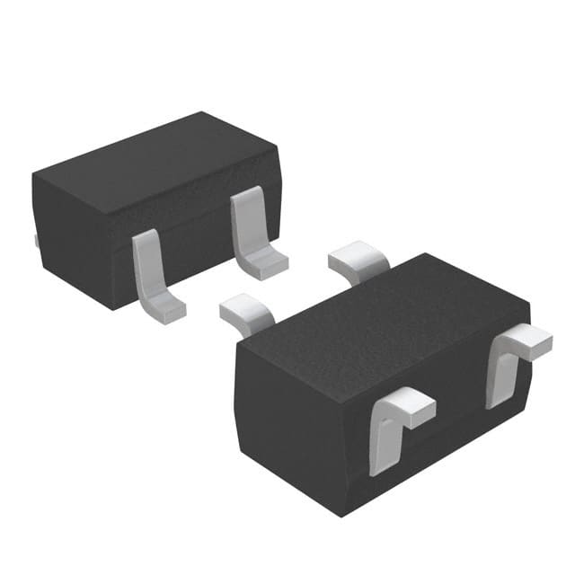
Package
XC6109C39ANR-G is available in a small surface mount package, which makes it suitable for compact electronic devices.
Essence
The essence of XC6109C39ANR-G lies in its ability to regulate voltage and manage power efficiently, ensuring stable and reliable operation of electronic devices.
Packaging/Quantity
This product is typically packaged in reels or tubes, with a quantity of 2500 units per reel/tube.
Specifications
- Input Voltage Range: 2.5V - 6.0V
- Output Voltage: 3.9V
- Output Current: Up to 100mA
- Dropout Voltage: 200mV (typical)
- Quiescent Current: 30μA (typical)
- Operating Temperature Range: -40°C to +85°C
Detailed Pin Configuration
- VIN: Input voltage pin
- GND: Ground pin
- VOUT: Output voltage pin
- EN: Enable pin (optional)
Functional Features
- Voltage regulation: XC6109C39ANR-G ensures a stable output voltage regardless of input voltage fluctuations.
- Power management: It efficiently manages power consumption, reducing energy waste.
- Enable pin: The optional enable pin allows for easy control of the device's operation.
Advantages and Disadvantages
Advantages
- High efficiency: The XC6109C39ANR-G operates with high efficiency, minimizing power loss.
- Compact size: Its small package size makes it suitable for space-constrained applications.
- Low power consumption: The quiescent current of 30μA ensures minimal power usage when the device is in standby mode.
Disadvantages
- Limited output current: The maximum output current of 100mA may not be sufficient for high-power applications.
- Dropout voltage: The 200mV dropout voltage may affect performance in low input voltage scenarios.
Working Principles
XC6109C39ANR-G utilizes a combination of internal circuitry and feedback mechanisms to regulate the output voltage. It compares the actual output voltage with a reference voltage and adjusts the internal circuitry accordingly to maintain a stable output.
Detailed Application Field Plans
XC6109C39ANR-G finds applications in various electronic devices, including but not limited to: - Mobile phones - Portable media players - Digital cameras - Wearable devices - IoT devices
Detailed and Complete Alternative Models
- XC6109C39ANR-G-XX: Similar to XC6109C39ANR-G, but with extended temperature range (-40°C to +125°C).
- XC6109C39ANR-G-YY: Improved version with lower dropout voltage (150mV) and higher output current (150mA).
These alternative models provide options for different operating conditions and specific requirements.
Word count: 346 words
Sebutkan 10 pertanyaan dan jawaban umum terkait penerapan XC6109C39ANR-G dalam solusi teknis
Sure! Here are 10 common questions and answers related to the application of XC6109C39ANR-G in technical solutions:
1. What is XC6109C39ANR-G? - XC6109C39ANR-G is a voltage detector IC (Integrated Circuit) that monitors the power supply voltage and provides a reset signal when the voltage drops below a certain threshold.
2. What is the operating voltage range of XC6109C39ANR-G? - The operating voltage range of XC6109C39ANR-G is typically between 0.8V and 6.0V.
3. What is the purpose of using XC6109C39ANR-G in a technical solution? - XC6109C39ANR-G is commonly used to monitor the power supply voltage in various electronic devices and systems, ensuring proper operation and preventing damage due to voltage fluctuations.
4. How does XC6109C39ANR-G provide a reset signal? - When the voltage drops below the specified threshold, XC6109C39ANR-G pulls its RESET pin low, indicating a reset condition to the microcontroller or other components in the system.
5. Can XC6109C39ANR-G be used in battery-powered applications? - Yes, XC6109C39ANR-G can be used in battery-powered applications as it operates within a wide voltage range and consumes very low quiescent current.
6. What is the typical accuracy of the voltage detection in XC6109C39ANR-G? - The typical accuracy of voltage detection in XC6109C39ANR-G is ±1.5%.
7. Does XC6109C39ANR-G have any built-in delay time for the reset signal? - Yes, XC6109C39ANR-G has a built-in delay time of approximately 200ms to ensure stable power supply before releasing the reset signal.
8. Can XC6109C39ANR-G be used in automotive applications? - Yes, XC6109C39ANR-G is suitable for automotive applications as it meets the AEC-Q100 Grade 2 qualification standards.
9. What is the package type of XC6109C39ANR-G? - XC6109C39ANR-G is available in a compact SOT-23-5 package.
10. Are there any specific precautions to consider when using XC6109C39ANR-G? - It is important to follow the recommended operating conditions and application circuit guidelines provided in the datasheet of XC6109C39ANR-G. Additionally, proper decoupling capacitors should be used near the VDD and GND pins for stable operation.