

Lihat spesifikasi untuk detail produk.
TLC5510INSR
Product Overview
Category
TLC5510INSR belongs to the category of integrated circuits (ICs).
Use
This IC is commonly used for analog-to-digital conversion in various electronic devices.
Characteristics
- High precision: TLC5510INSR offers high-resolution analog-to-digital conversion, ensuring accurate measurement and data acquisition.
- Low power consumption: The IC is designed to operate efficiently with minimal power consumption, making it suitable for battery-powered applications.
- Wide voltage range: It can handle a wide input voltage range, allowing flexibility in different operating conditions.
- Small package size: The IC comes in a compact package, enabling space-saving designs in electronic systems.
- Easy integration: TLC5510INSR can be easily integrated into existing circuitry due to its compatibility with standard digital interfaces.
Package and Quantity
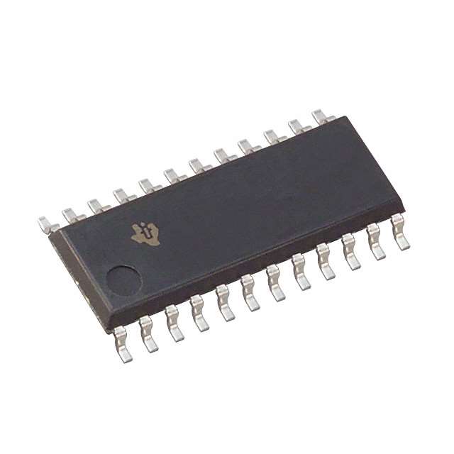
The TLC5510INSR is available in a small outline integrated circuit (SOIC) package. Each package contains one IC.
Specifications
- Resolution: 10 bits
- Input voltage range: 0V to Vref
- Supply voltage: 2.7V to 5.5V
- Conversion rate: 200 kilosamples per second (ksps)
- Operating temperature range: -40°C to +85°C
- Interface: Serial Peripheral Interface (SPI)
Pin Configuration
The TLC5510INSR has a total of 16 pins, which are assigned specific functions as follows:
- Vref: Reference voltage input
- AGND: Analog ground
- VIN: Analog input voltage
- CLK: Clock input for SPI communication
- CS: Chip select input
- DOUT: Digital output
- DIN: Serial data input
- DGND: Digital ground
- NC: No connection
- NC: No connection
- NC: No connection
- NC: No connection
- NC: No connection
- NC: No connection
- VCC: Supply voltage
- NC: No connection
Functional Features
- High-resolution conversion: The TLC5510INSR provides 10-bit resolution, ensuring accurate digitization of analog signals.
- Serial communication interface: It utilizes the SPI protocol for easy integration with microcontrollers and other digital devices.
- Low power consumption: The IC operates efficiently with low power consumption, making it suitable for battery-powered applications.
- Internal reference voltage: It includes an internal reference voltage source, eliminating the need for an external reference.
Advantages and Disadvantages
Advantages
- High precision and accuracy in analog-to-digital conversion.
- Low power consumption extends battery life in portable devices.
- Compact package size allows for space-saving designs.
- Easy integration with existing circuitry due to standard digital interface compatibility.
Disadvantages
- Limited resolution compared to higher-end ADCs.
- Restricted input voltage range may not be suitable for certain applications requiring wider dynamic range.
Working Principles
The TLC5510INSR operates on the principle of successive approximation. It samples the analog input voltage and converts it into a digital representation using a series of comparisons and adjustments. The internal reference voltage sets the upper limit for the input voltage range. The conversion process is controlled by the clock signal provided through the SPI interface.
Application Field Plans
The TLC5510INSR finds application in various fields, including: 1. Industrial automation: Used for precise measurement and control in industrial processes. 2. Medical devices: Enables accurate data acquisition in medical equipment such as patient monitors. 3. Test and measurement instruments: Provides high-resolution analog-to-digital conversion for accurate measurements. 4. Consumer electronics: Used in audio systems, instrumentation, and other consumer electronic devices requiring analog-to-digital conversion.
Alternative Models
- ADC0804: 8-bit analog-to-digital converter with similar features and interface.
- ADS1115: 16-bit analog-to-digital converter with higher resolution and extended input voltage range.
- MCP3208: 12-bit analog-to-digital converter with SPI interface and multiple input channels.
These alternative models offer different resolutions, input voltage ranges, and additional features to suit specific application requirements.
Word count: 536 words
Sebutkan 10 pertanyaan dan jawaban umum terkait penerapan TLC5510INSR dalam solusi teknis
Sure! Here are 10 common questions and answers related to the application of TLC5510INSR in technical solutions:
Q: What is the TLC5510INSR? A: The TLC5510INSR is a 10-bit analog-to-digital converter (ADC) integrated circuit (IC) manufactured by Texas Instruments.
Q: What is the operating voltage range of the TLC5510INSR? A: The operating voltage range of the TLC5510INSR is typically between 2.7V and 5.5V.
Q: What is the maximum sampling rate of the TLC5510INSR? A: The TLC5510INSR has a maximum sampling rate of 200 kilosamples per second (ksps).
Q: What is the resolution of the TLC5510INSR? A: The TLC5510INSR has a resolution of 10 bits, which means it can represent analog input signals with 1024 discrete levels.
Q: Can the TLC5510INSR be used for both single-ended and differential measurements? A: Yes, the TLC5510INSR supports both single-ended and differential measurements, providing flexibility in various applications.
Q: Does the TLC5510INSR have an internal reference voltage? A: No, the TLC5510INSR does not have an internal reference voltage. An external reference voltage must be provided for accurate conversions.
Q: What is the power consumption of the TLC5510INSR? A: The power consumption of the TLC5510INSR depends on the operating conditions, but it typically ranges from 1mW to 10mW.
Q: Can the TLC5510INSR operate in a low-power mode? A: Yes, the TLC5510INSR has a low-power mode that can be enabled to reduce power consumption during idle periods.
Q: What is the interface used to communicate with the TLC5510INSR? A: The TLC5510INSR uses a serial interface called Serial Peripheral Interface (SPI) for communication with a microcontroller or other devices.
Q: Are there any evaluation boards or development kits available for the TLC5510INSR? A: Yes, Texas Instruments provides evaluation boards and development kits that include the TLC5510INSR, allowing engineers to quickly prototype and test their designs.
Please note that these answers are general and may vary depending on specific datasheet specifications and application requirements.