

Lihat spesifikasi untuk detail produk.
TLC540IFNR
Product Overview
Category
TLC540IFNR belongs to the category of integrated circuits (ICs).
Use
This IC is commonly used in electronic devices for signal conditioning and amplification.
Characteristics
- TLC540IFNR is a low-power, high-performance operational amplifier.
- It operates on a single power supply voltage ranging from 2.7V to 5.5V.
- The IC has a rail-to-rail input and output capability.
- It offers a wide bandwidth and low input offset voltage.
- TLC540IFNR is designed for applications requiring precision amplification.
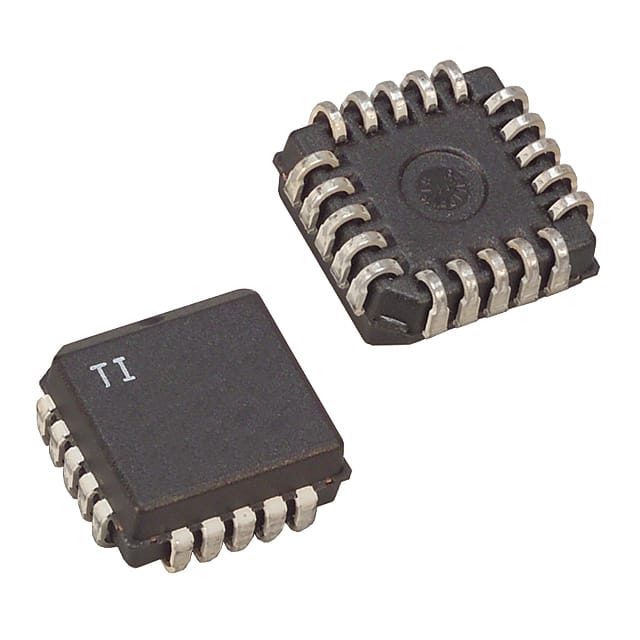
Package
The TLC540IFNR is available in a small outline package (SOIC) with 8 pins.
Essence
The essence of TLC540IFNR lies in its ability to provide accurate and reliable amplification of signals in various electronic devices.
Packaging/Quantity
The IC is typically sold in reels or tubes containing multiple units. The exact quantity may vary depending on the supplier.
Specifications
- Supply Voltage: 2.7V to 5.5V
- Input Offset Voltage: ±1mV (maximum)
- Gain Bandwidth Product: 10MHz (typical)
- Slew Rate: 3.5V/µs (typical)
- Input Bias Current: ±1pA (maximum)
- Operating Temperature Range: -40°C to +125°C
Detailed Pin Configuration
The TLC540IFNR IC has the following pin configuration:
- V-
- IN-
- IN+
- V+
- OUT
- NC (No Connection)
- NC (No Connection)
- VREF
Functional Features
- Rail-to-rail input and output operation allows for maximum dynamic range.
- Low input offset voltage ensures accurate signal amplification.
- High gain bandwidth product enables amplification of high-frequency signals.
- Low power consumption makes it suitable for battery-powered devices.
- Wide operating temperature range allows for use in various environments.
Advantages and Disadvantages
Advantages
- High precision amplification
- Wide bandwidth
- Low input offset voltage
- Rail-to-rail operation
- Low power consumption
Disadvantages
- Limited number of pins for additional functionalities
- Not suitable for applications requiring high voltage amplification
Working Principles
TLC540IFNR operates as a voltage amplifier by taking an input signal and amplifying it to a higher level. It utilizes internal circuitry to provide accurate amplification while maintaining low power consumption. The rail-to-rail input and output capability ensures that the amplified signal remains within the desired voltage range.
Detailed Application Field Plans
TLC540IFNR is commonly used in the following applications:
- Sensor signal conditioning
- Audio amplification
- Portable instrumentation
- Battery-powered devices
- Communication systems
Detailed and Complete Alternative Models
Some alternative models to TLC540IFNR include:
- LM358: Dual operational amplifier with similar characteristics.
- MCP6002: Low-power, rail-to-rail input/output operational amplifier.
- AD8605: Precision, low-power CMOS operational amplifier.
These alternative models offer similar functionality and can be used as substitutes depending on specific requirements.
Word count: 369 words
Sebutkan 10 pertanyaan dan jawaban umum terkait penerapan TLC540IFNR dalam solusi teknis
Sure! Here are 10 common questions and answers related to the application of TLC540IFNR in technical solutions:
Q: What is TLC540IFNR? A: TLC540IFNR is a specific model of an integrated circuit (IC) designed for use in technical solutions, particularly in analog-to-digital converters (ADCs).
Q: What is the purpose of TLC540IFNR? A: The purpose of TLC540IFNR is to convert analog signals into digital data, making it suitable for applications that require precise measurement and control.
Q: What are the key features of TLC540IFNR? A: Some key features of TLC540IFNR include low power consumption, high accuracy, wide operating voltage range, and compatibility with various microcontrollers.
Q: How does TLC540IFNR work? A: TLC540IFNR works by sampling and quantizing analog input signals, then converting them into digital values using its built-in ADC circuitry.
Q: What is the resolution of TLC540IFNR? A: TLC540IFNR has a resolution of 8 bits, meaning it can represent analog signals with 256 discrete levels.
Q: Can TLC540IFNR handle multiple channels? A: No, TLC540IFNR is a single-channel ADC, which means it can only process one analog signal at a time.
Q: What is the maximum sampling rate of TLC540IFNR? A: The maximum sampling rate of TLC540IFNR is typically around 20 kilosamples per second (ksps), allowing for real-time data acquisition in many applications.
Q: Is TLC540IFNR suitable for low-power applications? A: Yes, TLC540IFNR is designed to operate with low power consumption, making it suitable for battery-powered or energy-efficient devices.
Q: Can TLC540IFNR be used with different microcontrollers? A: Yes, TLC540IFNR is compatible with various microcontrollers and can communicate using standard digital interfaces such as SPI or I2C.
Q: What are some typical applications of TLC540IFNR? A: Some typical applications of TLC540IFNR include sensor interfacing, data acquisition systems, industrial automation, medical devices, and instrumentation.