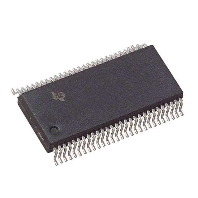
Lihat spesifikasi untuk detail produk.

SN74LVCH16652ADLR
Product Overview
- Category: Integrated Circuit (IC)
- Use: Data transmission and storage
- Characteristics: High-speed, low-voltage, 16-bit bus transceiver with 3-state outputs
- Package: TSSOP (Thin Shrink Small Outline Package)
- Essence: Transceiver IC for bidirectional data communication between two buses
- Packaging/Quantity: Reel packaging, 2500 units per reel
Specifications
- Logic Family: LVCH
- Number of Bits: 16
- Supply Voltage Range: 1.65V to 3.6V
- Input/Output Voltage Levels: Compatible with both TTL and CMOS levels
- Maximum Operating Frequency: 200 MHz
- Output Drive Strength: ±24 mA
- Operating Temperature Range: -40°C to +85°C
Detailed Pin Configuration
The SN74LVCH16652ADLR has a total of 56 pins, which are divided into various functional groups:
- VCC: Power supply pins (+3.3V)
- GND: Ground pins (0V)
- A1-A16: Inputs from Bus A
- B1-B16: Inputs from Bus B
- DIR: Direction control input
- OE: Output enable input
- Y1-Y16: Outputs to Bus A
- Z1-Z16: Outputs to Bus B
Functional Features
- Bidirectional Data Transmission: Allows data to be transmitted in both directions between Bus A and Bus B.
- 3-State Outputs: The outputs can be put in a high-impedance state, allowing multiple devices to share the same bus without interference.
- Direction Control: The DIR pin determines the direction of data flow.
- Output Enable: The OE pin enables or disables the outputs.
Advantages and Disadvantages
Advantages: - High-speed operation - Low-voltage operation - 3-state outputs for bus sharing - Wide operating temperature range
Disadvantages: - Limited to 16-bit data transmission - Requires external control signals for direction and output enable
Working Principles
The SN74LVCH16652ADLR is a bidirectional transceiver that facilitates data communication between two buses. The direction of data flow is controlled by the DIR pin, while the OE pin enables or disables the outputs. The IC operates at high speeds and low voltages, making it suitable for various applications.
Detailed Application Field Plans
The SN74LVCH16652ADLR can be used in a wide range of applications, including:
- Data Communication Systems: Enables bidirectional data transfer between different subsystems.
- Memory Modules: Facilitates data transmission between memory modules and other components.
- Industrial Automation: Allows communication between various control units and sensors.
- Networking Equipment: Supports data exchange between networking devices.
- Automotive Electronics: Enables data transfer between different automotive systems.
Detailed and Complete Alternative Models
- SN74LVCH16652A: Similar functionality but with different package options (SSOP, TSSOP, SOIC).
- MC74LVX16652: Equivalent transceiver IC from a different manufacturer.
- 74HC16652: CMOS-based alternative with similar specifications.
(Note: This list is not exhaustive and there may be other alternative models available in the market.)
This encyclopedia entry provides an overview of the SN74LVCH16652ADLR, including its product details, specifications, pin configuration, functional features, advantages, disadvantages, working principles, application field plans, and alternative models.
Sebutkan 10 pertanyaan dan jawaban umum terkait penerapan SN74LVCH16652ADLR dalam solusi teknis
Sure! Here are 10 common questions and answers related to the application of SN74LVCH16652ADLR in technical solutions:
Q: What is SN74LVCH16652ADLR? A: SN74LVCH16652ADLR is a 16-bit universal bus transceiver with 3-state outputs, designed for low-voltage (LV) applications.
Q: What is the voltage range supported by SN74LVCH16652ADLR? A: SN74LVCH16652ADLR supports a voltage range of 1.65V to 3.6V.
Q: What is the purpose of a bus transceiver? A: A bus transceiver is used to enable bidirectional data transfer between two buses or systems.
Q: How many bits can SN74LVCH16652ADLR handle? A: SN74LVCH16652ADLR can handle 16 bits of data.
Q: Can SN74LVCH16652ADLR be used in both input and output modes? A: Yes, SN74LVCH16652ADLR can be used as both an input and output device.
Q: What is the maximum data rate supported by SN74LVCH16652ADLR? A: SN74LVCH16652ADLR supports a maximum data rate of 200 MHz.
Q: Does SN74LVCH16652ADLR have built-in ESD protection? A: Yes, SN74LVCH16652ADLR has built-in ESD protection to safeguard against electrostatic discharge.
Q: Can SN74LVCH16652ADLR be used in hot-swapping applications? A: Yes, SN74LVCH16652ADLR supports hot-swapping, allowing for the insertion and removal of devices without disrupting the system.
Q: What is the power supply voltage required for SN74LVCH16652ADLR? A: SN74LVCH16652ADLR requires a power supply voltage of 1.65V to 3.6V.
Q: Are there any special considerations when designing with SN74LVCH16652ADLR? A: It is important to ensure proper decoupling and bypassing techniques are used to minimize noise and ensure stable operation. Additionally, attention should be given to signal integrity and impedance matching when working with high-speed data signals.
Please note that these answers are general and may vary depending on specific application requirements.

