

Lihat spesifikasi untuk detail produk.
SN74LVC2G126YZPR
Basic Information Overview
- Category: Integrated Circuit (IC)
- Use: Logic Gate Buffer/Driver
- Characteristics:
- Low-voltage CMOS technology
- Dual gate buffer/driver
- High-speed operation
- Wide operating voltage range
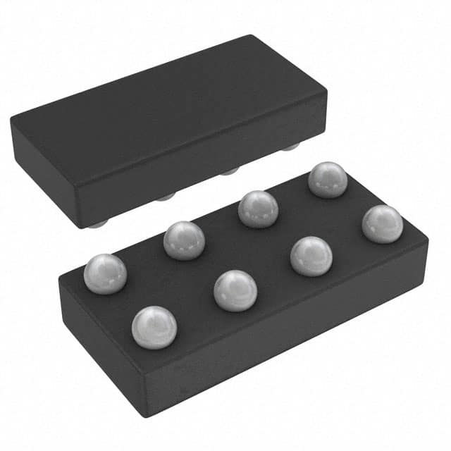
- Package: 8-pin small-outline integrated circuit (SOIC)
- Essence: Buffering and driving signals in digital circuits
- Packaging/Quantity: Tape and reel, 2500 units per reel
Specifications
- Supply Voltage Range: 1.65V to 5.5V
- Input Voltage Range: 0V to VCC
- Output Voltage Range: 0V to VCC
- Operating Temperature Range: -40°C to +85°C
- Maximum Propagation Delay Time: 4.3ns
- Maximum Quiescent Current: 10μA
Detailed Pin Configuration
The SN74LVC2G126YZPR has the following pin configuration:
___________
   1 |             | 8
   2 |             | 7
   3 |             | 6
   4 |             | 5
     |_____________|
Pin Description: 1. A Input 1 2. Y Output 1 3. GND Ground 4. Y Output 2 5. B Input 2 6. VCC Power Supply 7. OE Output Enable 8. NC No Connection
Functional Features
- Dual gate buffer/driver with independent control
- Provides buffering and driving capabilities for digital signals
- Supports bidirectional data flow
- High-speed operation allows for efficient signal transmission
- Wide operating voltage range enables compatibility with various systems
Advantages and Disadvantages
Advantages: - Low-voltage CMOS technology ensures low power consumption - Dual gate design allows for independent control of each buffer/driver - High-speed operation facilitates fast signal propagation - Wide operating voltage range enhances versatility
Disadvantages: - Limited number of input/output channels (2 in this case) - Relatively small package size may limit heat dissipation capabilities
Working Principles
The SN74LVC2G126YZPR is a logic gate buffer/driver that operates using low-voltage CMOS technology. It consists of two independent buffer/driver circuits, each capable of buffering and driving digital signals. The device can be controlled by an output enable (OE) pin, which allows the user to enable or disable the outputs.
When the OE pin is high, the outputs are enabled, and the inputs are buffered and driven to the corresponding outputs. Conversely, when the OE pin is low, the outputs are disabled, and the inputs do not affect the outputs.
The device operates within a wide voltage range, allowing it to be used in various systems with different supply voltages. Its high-speed operation ensures efficient signal transmission, making it suitable for applications requiring fast data transfer.
Detailed Application Field Plans
The SN74LVC2G126YZPR is commonly used in the following application fields: 1. Microcontrollers and microprocessors 2. Communication systems 3. Data storage devices 4. Industrial automation 5. Automotive electronics
In microcontroller and microprocessor systems, the SN74LVC2G126YZPR can be used to buffer and drive signals between the processor and other peripheral devices, such as memory modules, display units, and input/output interfaces.
In communication systems, the device can be employed to interface between different components, ensuring proper signal levels and driving capabilities.
Data storage devices, such as solid-state drives (SSDs), often require signal buffering and driving to maintain data integrity during read and write operations. The SN74LVC2G126YZPR can fulfill this requirement effectively.
Industrial automation systems often involve the control and monitoring of various sensors and actuators. The SN74LVC2G126YZPR can be utilized to buffer and drive signals between the control unit and these devices.
Automotive electronics, including infotainment systems, navigation units, and engine control modules, can benefit from the buffering and driving capabilities of the SN74LVC2G126YZPR to ensure reliable signal transmission.
Detailed and Complete Alternative Models
- SN74LVC2G07: Dual Buffer/Driver with Open-Drain Outputs
- SN74LVC2G34: Dual Buffer/Driver with Schmitt-Trigger Inputs
- SN74LVC2G241: Dual Buffer/Driver with 3-State Outputs
- SN74LVC2G08: Dual AND Gate
These alternative models offer similar functionality to the SN74LVC2G126YZPR but may have different pin configurations, package options, or additional features depending on specific application requirements.
Word count: 607 words
Sebutkan 10 pertanyaan dan jawaban umum terkait penerapan SN74LVC2G126YZPR dalam solusi teknis
Sure! Here are 10 common questions and answers related to the application of SN74LVC2G126YZPR:
Q: What is SN74LVC2G126YZPR? A: SN74LVC2G126YZPR is a dual bus buffer gate with 3-state outputs, commonly used in digital logic applications.
Q: What is the operating voltage range for SN74LVC2G126YZPR? A: The operating voltage range for SN74LVC2G126YZPR is typically between 1.65V and 5.5V.
Q: What is the maximum output current that SN74LVC2G126YZPR can handle? A: SN74LVC2G126YZPR can handle a maximum output current of 32mA.
Q: Can SN74LVC2G126YZPR be used as a level shifter? A: Yes, SN74LVC2G126YZPR can be used as a level shifter to convert signals between different voltage levels.
Q: How many inputs does SN74LVC2G126YZPR have? A: SN74LVC2G126YZPR has two input pins, A and B.
Q: What is the propagation delay of SN74LVC2G126YZPR? A: The propagation delay of SN74LVC2G126YZPR is typically around 3.8ns.
Q: Can SN74LVC2G126YZPR be used in high-speed applications? A: Yes, SN74LVC2G126YZPR is designed for high-speed operation and can be used in such applications.
Q: Is SN74LVC2G126YZPR compatible with both CMOS and TTL logic levels? A: Yes, SN74LVC2G126YZPR is compatible with both CMOS and TTL logic levels.
Q: Can SN74LVC2G126YZPR be used in battery-powered applications? A: Yes, SN74LVC2G126YZPR can be used in battery-powered applications as it operates at low voltage levels.
Q: What is the package type for SN74LVC2G126YZPR? A: SN74LVC2G126YZPR is available in a small footprint 8-pin DSBGA package.