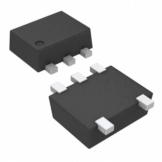
Lihat spesifikasi untuk detail produk.

SN74LVC1G34DRLR
Product Overview
- Category: Integrated Circuit
- Use: Logic Gate
- Characteristics: Single Buffer/Driver, Non-Inverting, 3-State Output
- Package: SOT-553
- Essence: High-Speed CMOS Technology
- Packaging/Quantity: Tape and Reel, 3000 pieces per reel
Specifications
- Supply Voltage Range: 1.65V to 5.5V
- Input Voltage Range: 0V to VCC
- Output Voltage Range: 0V to VCC
- Maximum Operating Frequency: 400 MHz
- Propagation Delay: 2.9 ns (typical)
- Output Drive Capability: ±24 mA
- Operating Temperature Range: -40°C to +85°C
Detailed Pin Configuration
The SN74LVC1G34DRLR has the following pin configuration:
____
   A |1    6| VCC
   Y |2    5| GND
   B |3    4| OE
       ----
Functional Features
- Single buffer/driver with non-inverting 3-state output
- High-speed operation suitable for various applications
- Supports wide supply voltage range for compatibility
- Low power consumption
- Schmitt-trigger input allows for noise immunity
- 3-state output allows multiple devices to share a bus
Advantages
- Compact size and low power consumption make it ideal for portable devices
- High-speed operation enables efficient data processing
- Wide supply voltage range provides flexibility in different applications
- Schmitt-trigger input ensures reliable operation in noisy environments
- 3-state output allows for easy bus sharing among multiple devices
Disadvantages
- Limited drive capability may not be suitable for high-current applications
- Only one logic gate function available in a single package
Working Principles
The SN74LVC1G34DRLR is a logic gate that operates using high-speed CMOS technology. It consists of a single buffer/driver with a non-inverting 3-state output. The input signal is processed by the Schmitt-trigger input, providing noise immunity and reliable operation even in noisy environments. The output can be enabled or disabled using the OE (Output Enable) pin, allowing multiple devices to share a bus.
Detailed Application Field Plans
The SN74LVC1G34DRLR is widely used in various applications, including:
- Portable electronic devices: Due to its compact size and low power consumption, it is commonly used in smartphones, tablets, and wearable devices.
- Communication systems: The high-speed operation makes it suitable for data transmission and reception in communication systems.
- Industrial automation: It can be utilized in control systems, sensors, and actuators for efficient data processing and signal conditioning.
- Automotive electronics: The wide supply voltage range and noise immunity make it suitable for automotive applications such as engine control units and infotainment systems.
Detailed and Complete Alternative Models
- SN74LVC1G04DBVR
- SN74LVC1G07DCKR
- SN74LVC1G08DCKR
- SN74LVC1G125DBVR
- SN74LVC1G126DBVR
- SN74LVC1G175DBVR
- SN74LVC1G240DBVR
- SN74LVC1G241DBVR
- SN74LVC1G32DBVR
- SN74LVC1G38DBVR
These alternative models offer similar functionality and characteristics to the SN74LVC1G34DRLR, providing options for different design requirements.
Word count: 310
Sebutkan 10 pertanyaan dan jawaban umum terkait penerapan SN74LVC1G34DRLR dalam solusi teknis
Sure! Here are 10 common questions and answers related to the application of SN74LVC1G34DRLR in technical solutions:
Q1: What is SN74LVC1G34DRLR? A1: SN74LVC1G34DRLR is a single buffer gate IC (Integrated Circuit) that provides a high-speed logic-level translation from one voltage level to another.
Q2: What is the operating voltage range of SN74LVC1G34DRLR? A2: The operating voltage range of SN74LVC1G34DRLR is from 1.65V to 5.5V.
Q3: What is the maximum output current of SN74LVC1G34DRLR? A3: The maximum output current of SN74LVC1G34DRLR is typically 32mA.
Q4: Can SN74LVC1G34DRLR be used for level shifting between different voltage domains? A4: Yes, SN74LVC1G34DRLR can be used for level shifting between different voltage domains as it supports bidirectional voltage translation.
Q5: What is the propagation delay of SN74LVC1G34DRLR? A5: The propagation delay of SN74LVC1G34DRLR is typically around 4.6ns.
Q6: Is SN74LVC1G34DRLR suitable for high-speed applications? A6: Yes, SN74LVC1G34DRLR is suitable for high-speed applications due to its fast propagation delay and high-speed operation.
Q7: Can SN74LVC1G34DRLR be used with both CMOS and TTL logic families? A7: Yes, SN74LVC1G34DRLR is compatible with both CMOS and TTL logic families, making it versatile for various applications.
Q8: Does SN74LVC1G34DRLR have built-in ESD protection? A8: Yes, SN74LVC1G34DRLR has built-in ESD (Electrostatic Discharge) protection, which helps protect the IC from damage during handling or operation.
Q9: What is the package type of SN74LVC1G34DRLR? A9: SN74LVC1G34DRLR comes in a small SOT-553 package, which is suitable for space-constrained designs.
Q10: Can SN74LVC1G34DRLR be used in battery-powered applications? A10: Yes, SN74LVC1G34DRLR can be used in battery-powered applications as it operates within a wide voltage range and has low power consumption.
Please note that these answers are general and may vary depending on specific application requirements.

