

Lihat spesifikasi untuk detail produk.
SN74LVC1G17DPWR
Basic Information Overview
- Category: Integrated Circuit (IC)
- Use: Logic Gate Buffer/Driver
- Characteristics:
- Low-voltage CMOS technology
- Single Schmitt-trigger buffer/driver
- Wide operating voltage range: 1.65V to 5.5V
- High-speed operation: 32 MHz typical
- Low power consumption
- Package: SOT-23-6
- Essence: Single-channel buffer with Schmitt-trigger input
- Packaging/Quantity: Tape and Reel, 2500 units per reel
Specifications
- Supply Voltage Range: 1.65V to 5.5V
- Input Voltage Range: 0V to VCC
- Output Voltage Range: 0V to VCC
- Operating Temperature Range: -40°C to +125°C
- Input Capacitance: 3.5pF
- Output Capacitance: 4.5pF
- Propagation Delay: 4.2ns (max) at 3.3V
- Output Drive Capability: ±24mA
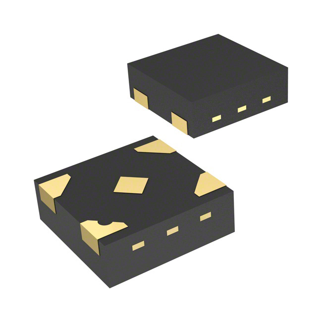
Detailed Pin Configuration
The SN74LVC1G17DPWR has a total of six pins arranged as follows:
____
   1 |o    | 6
   2 |     | 5
   3 |_____| 4
Pin Description: 1. A: Input (Schmitt-trigger) 2. GND: Ground 3. Y: Output 4. NC: No Connection 5. VCC: Power Supply 6. B: Input (Schmitt-trigger)
Functional Features
- Single Schmitt-trigger buffer/driver
- Converts slow input signals into fast output signals
- Provides hysteresis for improved noise immunity
- Allows interfacing between systems with different voltage levels
- Suitable for level shifting and signal buffering applications
Advantages
- Wide operating voltage range allows compatibility with various systems
- High-speed operation enables fast signal processing
- Low power consumption for energy-efficient designs
- Small package size (SOT-23-6) saves board space
- Schmitt-trigger input provides noise immunity and signal conditioning
Disadvantages
- Limited output drive capability compared to some other ICs
- Single-channel design may not be suitable for multi-channel applications
Working Principles
The SN74LVC1G17DPWR is a single-channel buffer/driver that utilizes a Schmitt-trigger input. It operates by converting slow input signals into fast output signals, providing hysteresis for improved noise immunity. The device can accept input voltages ranging from 0V to VCC and produces corresponding output voltages within the same range. It is designed to operate in a wide supply voltage range of 1.65V to 5.5V, making it compatible with various systems.
Detailed Application Field Plans
The SN74LVC1G17DPWR can be used in a variety of applications, including but not limited to: - Level shifting between different voltage domains - Signal buffering and amplification - Noise filtering and signal conditioning - Interface protection against voltage spikes and noise - Clock signal distribution and fan-out - Sensor signal conditioning and amplification - Battery-powered devices with low-power requirements
Detailed and Complete Alternative Models
Some alternative models that offer similar functionality to the SN74LVC1G17DPWR include: - SN74LVC1G07DBVR: Single-buffer gate with open-drain output - SN74LVC1G125DBVR: Single-buffer gate with tri-state output - SN74LVC1G240DBVR: Single-buffer gate with non-inverting output - SN74LVC1G32DBVR: Single 2-input OR gate
These alternative models can be considered based on specific application requirements and design constraints.
Word count: 446 words
Sebutkan 10 pertanyaan dan jawaban umum terkait penerapan SN74LVC1G17DPWR dalam solusi teknis
Sure! Here are 10 common questions and answers related to the application of SN74LVC1G17DPWR:
Q1: What is SN74LVC1G17DPWR? A1: SN74LVC1G17DPWR is a single Schmitt-trigger buffer/driver with open-drain output, commonly used in digital logic circuits.
Q2: What is the operating voltage range for SN74LVC1G17DPWR? A2: The operating voltage range for SN74LVC1G17DPWR is typically between 1.65V and 5.5V.
Q3: What is the maximum output current of SN74LVC1G17DPWR? A3: The maximum output current of SN74LVC1G17DPWR is typically 32mA.
Q4: Can SN74LVC1G17DPWR be used as a level shifter? A4: Yes, SN74LVC1G17DPWR can be used as a level shifter to convert signals between different voltage levels.
Q5: What is the maximum propagation delay of SN74LVC1G17DPWR? A5: The maximum propagation delay of SN74LVC1G17DPWR is typically 6.5ns.
Q6: Can SN74LVC1G17DPWR drive capacitive loads? A6: Yes, SN74LVC1G17DPWR can drive capacitive loads up to a certain limit specified in the datasheet.
Q7: Is SN74LVC1G17DPWR suitable for high-speed applications? A7: Yes, SN74LVC1G17DPWR is designed for high-speed operation and can be used in various high-frequency applications.
Q8: Does SN74LVC1G17DPWR have built-in ESD protection? A8: Yes, SN74LVC1G17DPWR has built-in ESD protection to safeguard against electrostatic discharge.
Q9: Can SN74LVC1G17DPWR be used in battery-powered applications? A9: Yes, SN74LVC1G17DPWR is suitable for battery-powered applications due to its low power consumption.
Q10: What is the package type of SN74LVC1G17DPWR? A10: SN74LVC1G17DPWR is available in a small SOT-23-5 package, which is commonly used for surface-mount applications.
Please note that these answers are general and may vary depending on the specific requirements and conditions of your technical solution. It's always recommended to refer to the datasheet and consult with the manufacturer for accurate information.