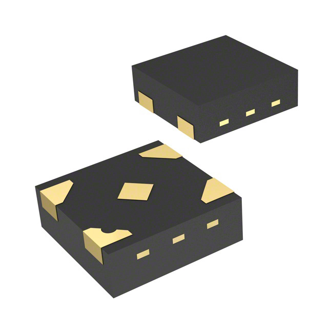
Lihat spesifikasi untuk detail produk.

SN74LVC1G08DPWR
Basic Information Overview
- Category: Integrated Circuit (IC)
- Use: Logic Gate
- Characteristics:
- Low-voltage CMOS technology
- Single 2-input AND gate
- High-speed operation
- Low power consumption
- Package: SOT-23-5
- Essence: Single-gate logic IC
- Packaging/Quantity: Tape and Reel, 3000 pieces per reel
Specifications
- Supply Voltage Range: 1.65V to 5.5V
- Input Voltage Range: 0V to VCC
- Output Voltage Range: 0V to VCC
- Operating Temperature Range: -40°C to +125°C
- Propagation Delay: 3.8 ns (typical) at 3.3V
- Maximum Quiescent Current: 1 μA at 5.5V
- Maximum Output Current: ±32 mA
Detailed Pin Configuration
The SN74LVC1G08DPWR has a total of 5 pins arranged as follows:
____
   Y --|    |-- VCC
   A --|    |-- B
 GND --|____|-- NC
- Y: Output pin
- A, B: Input pins
- VCC: Positive power supply
- GND: Ground
- NC: No connection (unused pin)
Functional Features
- Single 2-input AND gate functionality
- High-speed operation allows for quick signal processing
- Low power consumption makes it suitable for battery-powered devices
- Compatible with various voltage levels due to its wide supply voltage range
Advantages
- Small form factor and low pin count make it ideal for space-constrained applications
- Low power consumption extends battery life in portable devices
- High-speed operation enables efficient signal processing
- Wide supply voltage range allows for compatibility with different systems
Disadvantages
- Limited to a single 2-input AND gate functionality
- May not be suitable for complex logic operations requiring multiple gates
Working Principles
The SN74LVC1G08DPWR is based on low-voltage CMOS technology. It operates as a 2-input AND gate, where the output (Y) is high only when both inputs (A and B) are high. The IC uses a combination of transistors and logic gates to perform this logical operation.
Detailed Application Field Plans
The SN74LVC1G08DPWR finds applications in various fields, including: 1. Consumer Electronics: Used in smartphones, tablets, and wearable devices for logic operations. 2. Automotive: Employed in automotive electronics for signal processing and control functions. 3. Industrial Automation: Integrated into industrial control systems for logic operations and signal conditioning. 4. Communication Systems: Utilized in networking equipment and telecommunications devices for data processing.
Detailed and Complete Alternative Models
- SN74LVC1G00DBVR: Single 2-input NAND gate in SOT-23-5 package.
- SN74LVC1G02DCKR: Single 2-input NOR gate in SC-70-5 package.
- SN74LVC1G04DCKR: Single inverter (NOT gate) in SC-70-5 package.
- SN74LVC1G86DBVR: Single 2-input XOR gate in SOT-23-5 package.
These alternative models offer similar functionality but differ in terms of specific logic operations and package types.
In conclusion, the SN74LVC1G08DPWR is a single-gate logic IC belonging to the integrated circuit category. It is widely used for logic operations in various electronic devices. With its high-speed operation, low power consumption, and compatibility with different voltage levels, it offers advantages in terms of performance and flexibility. However, its limited functionality as a single 2-input AND gate may restrict its use in complex logic operations.
Sebutkan 10 pertanyaan dan jawaban umum terkait penerapan SN74LVC1G08DPWR dalam solusi teknis
Sure! Here are 10 common questions and answers related to the application of SN74LVC1G08DPWR:
1. What is SN74LVC1G08DPWR? SN74LVC1G08DPWR is a single 2-input AND gate IC (integrated circuit) that is commonly used in digital logic circuits.
2. What is the operating voltage range for SN74LVC1G08DPWR? The operating voltage range for SN74LVC1G08DPWR is typically between 1.65V and 5.5V.
3. What is the maximum output current of SN74LVC1G08DPWR? The maximum output current of SN74LVC1G08DPWR is around 32mA.
4. Can SN74LVC1G08DPWR be used as a level shifter? Yes, SN74LVC1G08DPWR can be used as a level shifter to convert signals from one voltage level to another.
5. What is the maximum propagation delay of SN74LVC1G08DPWR? The maximum propagation delay of SN74LVC1G08DPWR is typically around 4.3ns.
6. Is SN74LVC1G08DPWR suitable for high-speed applications? Yes, SN74LVC1G08DPWR is suitable for high-speed applications due to its low propagation delay and high-speed operation.
7. Can SN74LVC1G08DPWR be used in battery-powered devices? Yes, SN74LVC1G08DPWR can be used in battery-powered devices as it operates within a wide voltage range and has low power consumption.
8. What is the package type of SN74LVC1G08DPWR? SN74LVC1G08DPWR is available in a small SOT-23 package, which makes it suitable for space-constrained applications.
9. Can SN74LVC1G08DPWR be used in automotive applications? Yes, SN74LVC1G08DPWR is qualified for automotive applications and meets the necessary standards and requirements.
10. Are there any recommended application circuits available for SN74LVC1G08DPWR? Yes, the datasheet of SN74LVC1G08DPWR provides recommended application circuits that can help in designing with this IC.
Please note that these answers are general and may vary depending on specific design considerations and requirements. It is always recommended to refer to the datasheet and consult with technical experts for accurate information and guidance.

