Lihat spesifikasi untuk detail produk.

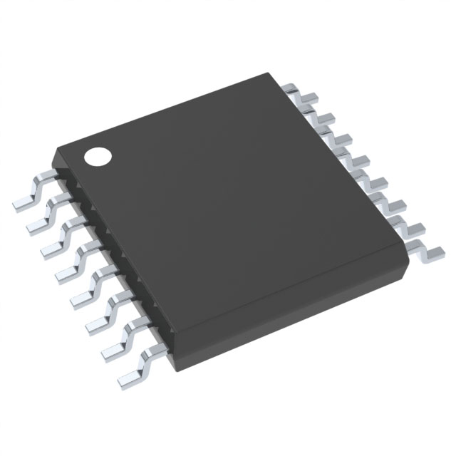
SN74LVC139APWG4
Product Overview
- Category: Integrated Circuit (IC)
- Use: Decoder/Demultiplexer
- Characteristics: Low-Voltage, CMOS Logic, Dual 2-Line to 4-Line Decoder/Demultiplexer
- Package: TSSOP-16
- Essence: High-performance digital logic device for decoding and demultiplexing applications
- Packaging/Quantity: Tape and Reel, 2500 units per reel
Specifications
- Supply Voltage Range: 1.65V to 5.5V
- High-Speed CMOS Technology
- Low Power Consumption: Max 10µA
- Schmitt-Trigger Inputs for Noise Immunity
- Output Drive Capability: ±24mA at 3.3V
- Operating Temperature Range: -40°C to +85°C
Detailed Pin Configuration
The SN74LVC139APWG4 has a total of 16 pins arranged as follows:
__    __
   A1 |1  `--' 16| VCC
   B1 |2        15| Y0
   A0 |3        14| Y1
   B0 |4        13| GND
   G1 |5        12| Y2
   G2 |6        11| Y3
   Y0 |7        10| B2
   Y1 |8         9| A2
       ``````````
Functional Features
- Dual 2-Line to 4-Line Decoder/Demultiplexer functionality
- Decodes two binary inputs into four mutually exclusive outputs
- Enables easy selection of one output from multiple inputs
- High-speed operation with low power consumption
- Schmitt-trigger inputs provide noise immunity
- Wide supply voltage range allows compatibility with various systems
Advantages and Disadvantages
Advantages: - High-speed operation - Low power consumption - Wide supply voltage range - Noise immunity with Schmitt-trigger inputs
Disadvantages: - Limited number of outputs (four) - Restricted input combinations due to binary decoding
Working Principles
The SN74LVC139APWG4 is a decoder/demultiplexer IC that takes two binary inputs (A1, A0) and selects one of the four outputs (Y0, Y1, Y2, Y3) based on the input combination. The G1 and G2 pins are used to enable or disable the device.
When both G1 and G2 are low, the outputs are enabled, and the selected output is determined by the binary input combination. When either G1 or G2 is high, all outputs are disabled.
The IC operates using high-speed CMOS technology, ensuring fast response times. The Schmitt-trigger inputs provide noise immunity, allowing reliable operation even in noisy environments.
Detailed Application Field Plans
The SN74LVC139APWG4 finds applications in various fields, including:
- Address Decoding: Used in microcontrollers and memory devices to decode address signals and select specific memory locations.
- Data Demultiplexing: Enables the selection of data from multiple sources and routing it to the desired destination.
- Signal Routing: Allows the routing of different signals to specific output channels based on the input combination.
- Control Circuitry: Used in control systems to decode control signals and activate specific functions based on the input combination.
Detailed and Complete Alternative Models
- 74HC139: Similar dual 2-line to 4-line decoder/demultiplexer IC with TTL logic levels.
- CD74HCT139E: Dual 2-to-4 line decoder/demultiplexer IC with Schmitt-trigger inputs and TTL logic levels.
- SN74LVC138A: 3-line to 8-line decoder/demultiplexer IC with similar characteristics but more output options.
These alternative models provide similar functionality and can be used as substitutes for the SN74LVC139APWG4 in various applications.
Word count: 420 words
Sebutkan 10 pertanyaan dan jawaban umum terkait penerapan SN74LVC139APWG4 dalam solusi teknis
Sure! Here are 10 common questions and answers related to the application of SN74LVC139APWG4 in technical solutions:
Q: What is SN74LVC139APWG4? A: SN74LVC139APWG4 is a dual 2-to-4 line decoder/demultiplexer integrated circuit (IC) that can be used in various digital logic applications.
Q: What is the operating voltage range for SN74LVC139APWG4? A: The operating voltage range for SN74LVC139APWG4 is typically between 1.65V and 5.5V.
Q: What is the maximum output current of SN74LVC139APWG4? A: The maximum output current per channel of SN74LVC139APWG4 is 32mA.
Q: Can SN74LVC139APWG4 be used as a demultiplexer? A: Yes, SN74LVC139APWG4 can be used as a demultiplexer by connecting its inputs to the select lines and using its outputs as separate channels.
Q: How many select lines does SN74LVC139APWG4 have? A: SN74LVC139APWG4 has two select lines, which can be used to control the decoding/demultiplexing operation.
Q: What is the propagation delay of SN74LVC139APWG4? A: The propagation delay of SN74LVC139APWG4 is typically around 4.7ns.
Q: Can SN74LVC139APWG4 be cascaded to increase the number of decoded outputs? A: Yes, multiple SN74LVC139APWG4 ICs can be cascaded together to increase the number of decoded outputs.
Q: Is SN74LVC139APWG4 compatible with both TTL and CMOS logic levels? A: Yes, SN74LVC139APWG4 is designed to be compatible with both TTL and CMOS logic levels.
Q: What is the package type for SN74LVC139APWG4? A: SN74LVC139APWG4 is available in a TSSOP (Thin Shrink Small Outline Package) package.
Q: Can SN74LVC139APWG4 be used in high-speed applications? A: Yes, SN74LVC139APWG4 is designed for high-speed operation and can be used in various high-frequency applications.
Please note that these answers are general and may vary depending on specific datasheet specifications and application requirements.

