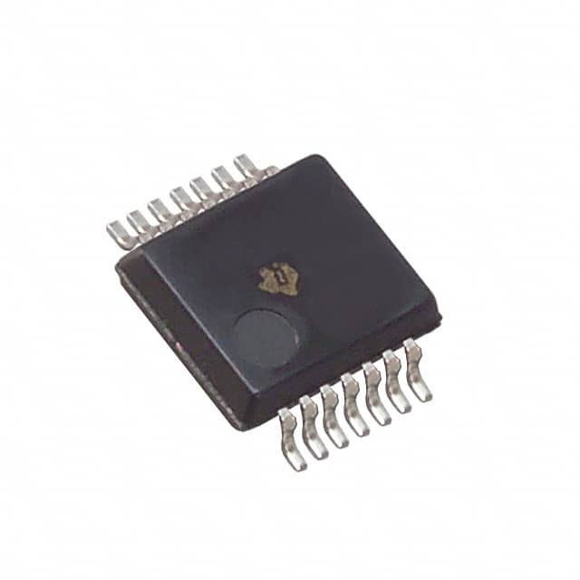
Lihat spesifikasi untuk detail produk.

SN74LV08ADBR
Product Overview
Category
SN74LV08ADBR belongs to the category of integrated circuits (ICs).
Use
This product is commonly used as a quad 2-input AND gate.
Characteristics
- Low voltage operation: SN74LV08ADBR operates at low voltages, typically between 1.65V and 5.5V.
- High-speed performance: It offers fast propagation delay times, making it suitable for applications requiring quick response times.
- Wide temperature range: The product can operate within a wide temperature range, typically from -40°C to 85°C.
- Low power consumption: SN74LV08ADBR consumes minimal power, making it energy-efficient.
Package
SN74LV08ADBR is available in a small-outline integrated circuit (SOIC) package.
Essence
The essence of SN74LV08ADBR lies in its ability to perform logical AND operations on two input signals.
Packaging/Quantity
This product is typically sold in reels or tubes containing multiple units. The exact quantity may vary depending on the supplier.
Specifications
- Supply Voltage Range: 1.65V to 5.5V
- Input Voltage Range: 0V to VCC
- Output Voltage Range: 0V to VCC
- Operating Temperature Range: -40°C to 85°C
- Propagation Delay Time: <10ns
- Maximum Operating Frequency: 100MHz
Detailed Pin Configuration
SN74LV08ADBR consists of 14 pins arranged as follows:
+---+--+---+
   A1  |1  +--+ 14| VCC
   B1  |2       13| C1
   A2  |3       12| B2
   B2  |4  SN74 11| A3
   Y1  |5  LV08 10| B3
   GND |6  AD   9| Y2
   Y2  |7       8| GND
       +----------+
Functional Features
- Quad 2-input AND gate: SN74LV08ADBR can perform logical AND operations on four sets of two input signals.
- High-speed operation: The product offers fast propagation delay times, enabling quick response in digital circuits.
- Low power consumption: SN74LV08ADBR consumes minimal power, making it suitable for battery-powered devices.
- Wide voltage range: It operates at low voltages, allowing compatibility with various electronic systems.
Advantages and Disadvantages
Advantages
- Low voltage operation enables compatibility with a wide range of electronic systems.
- Fast propagation delay times ensure quick response in digital circuits.
- Low power consumption makes it suitable for energy-efficient applications.
- Wide temperature range allows operation in extreme environmental conditions.
Disadvantages
- Limited to performing logical AND operations only.
- May not be suitable for applications requiring complex logic functions.
Working Principles
SN74LV08ADBR works based on the principles of digital logic. It takes two input signals and performs a logical AND operation on them. The output signal is high (logic 1) only when both input signals are high; otherwise, the output remains low (logic 0).
Detailed Application Field Plans
SN74LV08ADBR finds applications in various fields, including:
- Digital electronics: It is used in digital circuits to perform logical AND operations, enabling the implementation of complex logic functions.
- Microcontrollers and microprocessors: SN74LV08ADBR can be utilized as a building block for designing control units and data processing systems.
- Communication systems: It plays a crucial role in signal processing and filtering applications within communication systems.
- Industrial automation: The product is employed in industrial control systems for logical decision-making and signal conditioning.
Detailed and Complete Alternative Models
- SN74LV08ADR: Similar to SN74LV08ADBR, but available in a different package (SOIC-14).
- 74LV08: A compatible alternative from a different manufacturer, offering similar functionality and specifications.
- MC74LV08: Another alternative model with comparable features, manufactured by a different company.
These alternative models can be considered based on availability, pricing, and specific project requirements.
Word count: 550 words
Sebutkan 10 pertanyaan dan jawaban umum terkait penerapan SN74LV08ADBR dalam solusi teknis
Sure! Here are 10 common questions and answers related to the application of SN74LV08ADBR:
Q: What is SN74LV08ADBR? A: SN74LV08ADBR is a quad 2-input AND gate IC (integrated circuit) that is commonly used in digital logic applications.
Q: What is the operating voltage range of SN74LV08ADBR? A: The operating voltage range of SN74LV08ADBR is typically between 1.65V and 5.5V.
Q: What is the maximum output current of SN74LV08ADBR? A: The maximum output current of SN74LV08ADBR is 32mA per gate.
Q: Can SN74LV08ADBR be used for level shifting applications? A: Yes, SN74LV08ADBR can be used for level shifting applications as it supports both TTL and CMOS voltage levels.
Q: What is the propagation delay of SN74LV08ADBR? A: The propagation delay of SN74LV08ADBR is typically around 6 ns.
Q: Can SN74LV08ADBR be used in high-speed applications? A: Yes, SN74LV08ADBR can be used in high-speed applications as it has a fast switching speed.
Q: How many gates are there in SN74LV08ADBR? A: SN74LV08ADBR contains four independent 2-input AND gates.
Q: Is SN74LV08ADBR compatible with other logic families? A: Yes, SN74LV08ADBR is compatible with various logic families such as TTL, CMOS, and LVTTL.
Q: Can SN74LV08ADBR be used in battery-powered applications? A: Yes, SN74LV08ADBR can be used in battery-powered applications as it operates at low power consumption.
Q: What is the package type of SN74LV08ADBR? A: SN74LV08ADBR is available in a small-outline integrated circuit (SOIC) package.
Please note that these answers are general and may vary depending on specific datasheet specifications and application requirements.

