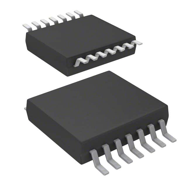
Lihat spesifikasi untuk detail produk.

SN74LV05ADGVR
Product Overview
Category
SN74LV05ADGVR belongs to the category of integrated circuits (ICs).
Use
It is commonly used as a hex inverter buffer/driver with open-drain outputs.
Characteristics
- Low-voltage operation: 2 V to 5.5 V
- High-speed performance: 4 ns propagation delay at 3.3 V
- Open-drain outputs for wired-AND applications
- Schmitt-trigger input allows for slow input transition and noise rejection
- Available in small package options for space-constrained applications
Package
SN74LV05ADGVR is available in a small SOT-23-6 package.
Essence
The essence of SN74LV05ADGVR lies in its ability to invert and buffer signals while providing open-drain outputs, making it suitable for wired-AND applications.
Packaging/Quantity
SN74LV05ADGVR is typically packaged in reels, with 3000 units per reel.
Specifications
- Supply voltage range: 2 V to 5.5 V
- Input voltage range: -0.5 V to VCC + 0.5 V
- Output voltage range: -0.5 V to VCC + 0.5 V
- Operating temperature range: -40°C to 85°C
- Maximum input current: ±1 mA
- Maximum output current: ±8 mA
Detailed Pin Configuration
SN74LV05ADGVR has a total of six pins arranged as follows:
____
   Y1 |    | VCC
   A1 |    | Y2
   A2 |    | GND
   Y3 |    | A3
   A4 |    | Y4
   Y5 |____| A5
Functional Features
- Hex inverter buffer/driver with open-drain outputs
- Schmitt-trigger input for noise rejection and slow input transition
- Low-voltage operation suitable for battery-powered applications
- High-speed performance for quick signal processing
Advantages and Disadvantages
Advantages
- Low-voltage operation allows for compatibility with a wide range of systems
- Open-drain outputs enable wired-AND applications
- Schmitt-trigger input enhances noise rejection and slow input transition handling
- Small package size suitable for space-constrained designs
Disadvantages
- Limited output current capacity may restrict use in high-current applications
- Not suitable for applications requiring high-speed data transmission
Working Principles
SN74LV05ADGVR operates by taking the input signal, inverting it, and buffering it to provide an output signal. The open-drain outputs allow multiple devices to be connected together in a wired-AND configuration. The Schmitt-trigger input ensures reliable operation even in the presence of noise or slow input transitions.
Detailed Application Field Plans
SN74LV05ADGVR finds applications in various fields, including but not limited to: 1. Battery-powered devices 2. Industrial automation 3. Consumer electronics 4. Automotive electronics 5. Communication systems
Detailed and Complete Alternative Models
Some alternative models that can be considered as alternatives to SN74LV05ADGVR are: 1. SN74LVC06A: Hex inverter buffer/driver with 5 V tolerant inputs 2. SN74AHC04: Hex inverter with high-speed performance 3. SN74HCT14: Hex Schmitt-trigger inverter for noise-sensitive applications
These alternative models offer similar functionality but may have different voltage ranges, speed characteristics, or additional features.
In conclusion, SN74LV05ADGVR is a versatile hex inverter buffer/driver with open-drain outputs. Its low-voltage operation, high-speed performance, and small package size make it suitable for a wide range of applications in various fields. However, its limited output current capacity and speed limitations should be considered when selecting the appropriate IC for specific requirements.
Sebutkan 10 pertanyaan dan jawaban umum terkait penerapan SN74LV05ADGVR dalam solusi teknis
Sure! Here are 10 common questions and answers related to the application of SN74LV05ADGVR:
Q: What is SN74LV05ADGVR? A: SN74LV05ADGVR is a hex inverter with open-drain outputs, which means it can invert input signals and drive them to an open-drain output.
Q: What is the voltage range supported by SN74LV05ADGVR? A: SN74LV05ADGVR supports a voltage range from 2 V to 5.5 V.
Q: Can SN74LV05ADGVR be used for level shifting between different voltage domains? A: Yes, SN74LV05ADGVR can be used for level shifting as it supports a wide voltage range.
Q: How many inverters are there in SN74LV05ADGVR? A: SN74LV05ADGVR has six inverters in a single package.
Q: What is the maximum current that SN74LV05ADGVR can sink or source? A: SN74LV05ADGVR can sink/source up to 32 mA of current per output.
Q: Can SN74LV05ADGVR handle high-speed signals? A: Yes, SN74LV05ADGVR is designed to handle high-speed signals with a propagation delay of around 7 ns.
Q: Is SN74LV05ADGVR suitable for bidirectional communication? A: No, SN74LV05ADGVR is not bidirectional. It only provides inversion and open-drain output functionality.
Q: Can SN74LV05ADGVR be used in automotive applications? A: Yes, SN74LV05ADGVR is suitable for automotive applications as it can operate in a wide temperature range (-40°C to 125°C).
Q: What is the package type of SN74LV05ADGVR? A: SN74LV05ADGVR comes in a small SOT-23-5 package.
Q: Are there any recommended decoupling capacitors for SN74LV05ADGVR? A: It is generally recommended to use a 0.1 µF ceramic capacitor placed close to the power supply pins of SN74LV05ADGVR for proper decoupling.
Please note that these answers are general and may vary depending on specific application requirements.

