

Lihat spesifikasi untuk detail produk.
SN74LS674N
Product Overview
- Category: Integrated Circuit (IC)
- Use: Logic Shift Register
- Characteristics:
- High-speed operation
- TTL compatible inputs and outputs
- Parallel or serial data entry
- Cascadable for larger shift registers
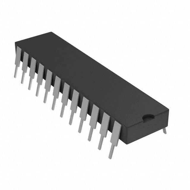
- Package: DIP (Dual In-line Package)
- Essence: The SN74LS674N is a 4-bit parallel or serial-in, serial-out shift register with asynchronous reset.
- Packaging/Quantity: Available in tubes of 25 units or reels of 2000 units.
Specifications
- Supply Voltage: 4.75V to 5.25V
- Operating Temperature Range: -40°C to +85°C
- Input Voltage High: 2.0V (min), 0.8V (max)
- Input Voltage Low: 0.8V (min), 0.4V (max)
- Output Voltage High: 2.7V (min), 3.4V (max)
- Output Voltage Low: 0.5V (max)
Detailed Pin Configuration
The SN74LS674N has a total of 16 pins:
- SER (Serial Data Input)
- P/S (Parallel/Serial Select)
- CLK (Clock Input)
- RST (Reset Input)
- QA (Output A)
- QB (Output B)
- QC (Output C)
- QD (Output D)
- GND (Ground)
- VCC (Supply Voltage)
- QA' (Complementary Output A)
- QB' (Complementary Output B)
- QC' (Complementary Output C)
- QD' (Complementary Output D)
- QH (Output High Impedance)
- QH' (Complementary Output High Impedance)
Functional Features
- Parallel or serial data entry: The SN74LS674N can accept data in parallel or serial format, providing flexibility in data input.
- Cascadable for larger shift registers: Multiple SN74LS674N devices can be cascaded together to create larger shift registers with increased storage capacity.
- Asynchronous reset: The device includes an asynchronous reset input (RST) that allows the register to be cleared at any time, independently of the clock signal.
Advantages and Disadvantages
Advantages: - High-speed operation: The SN74LS674N is designed for high-speed applications, making it suitable for time-critical tasks. - TTL compatible inputs and outputs: The device is compatible with TTL logic levels, allowing easy integration into existing systems. - Flexible data input: The ability to accept data in parallel or serial format provides versatility in different application scenarios.
Disadvantages: - Limited storage capacity: As a 4-bit shift register, the SN74LS674N has a relatively small storage capacity compared to higher-bit counterparts. - Lack of built-in error detection/correction: The device does not include built-in error detection or correction mechanisms, requiring additional circuitry for such functionalities if needed.
Working Principles
The SN74LS674N operates based on the principles of sequential logic. It uses flip-flops to store and shift data bits. The clock signal controls the shifting of data from one flip-flop to another. The P/S input determines whether data is entered in parallel or serial mode. The RST input asynchronously resets the register, clearing all stored data.
Detailed Application Field Plans
The SN74LS674N can be used in various applications, including:
- Data communication systems
- Serial-to-parallel conversion
- Parallel-to-serial conversion
- Data storage and retrieval systems
- Shift register-based counters
Detailed and Complete Alternative Models
- SN74LS595N: 8-bit serial-in, parallel-out shift register
- SN74HC164N: 8-bit serial-in, parallel-out shift register
- CD4015BE: Dual 4-bit static shift register
- CD4021BE: 8-stage static shift register
- CD4094BE: 8-bit serial-in, parallel-out shift register with output latches
These alternative models offer similar functionality to the SN74LS674N and can be considered as alternatives based on specific requirements.
Word count: 446 words
Sebutkan 10 pertanyaan dan jawaban umum terkait penerapan SN74LS674N dalam solusi teknis
Sure! Here are 10 common questions and answers related to the application of SN74LS674N in technical solutions:
Q: What is SN74LS674N? A: SN74LS674N is a specific type of integrated circuit (IC) commonly used in digital electronics applications.
Q: What is the function of SN74LS674N? A: SN74LS674N is a 4-bit binary counter IC with parallel load capability, which means it can count up or down based on input signals.
Q: What voltage levels does SN74LS674N support? A: SN74LS674N operates at a supply voltage range of 4.75V to 5.25V.
Q: How many inputs and outputs does SN74LS674N have? A: SN74LS674N has 4 inputs (A, B, C, D) and 4 outputs (Q0, Q1, Q2, Q3).
Q: Can SN74LS674N be cascaded to create larger counters? A: Yes, multiple SN74LS674N ICs can be cascaded together to create larger counters with more bits.
Q: What is the maximum clock frequency supported by SN74LS674N? A: SN74LS674N can operate at a maximum clock frequency of 30 MHz.
Q: How do I load data into SN74LS674N? A: Data can be loaded into SN74LS674N by applying the desired binary values to the A, B, C, and D inputs and then pulsing the LOAD input.
Q: Can SN74LS674N be used as a frequency divider? A: Yes, SN74LS674N can be used as a frequency divider by connecting the clock input to a higher-frequency signal and using the outputs as divided frequencies.
Q: What is the power consumption of SN74LS674N? A: The power consumption of SN74LS674N varies depending on the operating conditions, but it typically ranges from 10mW to 25mW.
Q: Are there any specific precautions to consider when using SN74LS674N? A: Yes, some precautions include proper decoupling of power supply pins, avoiding excessive input voltage levels, and ensuring proper grounding to minimize noise interference.
Please note that these answers are general and may vary based on specific application requirements and datasheet specifications.