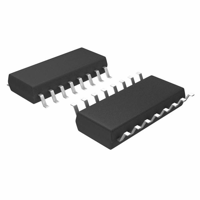
Lihat spesifikasi untuk detail produk.

SN74LS541DBRG4
Product Overview
- Category: Integrated Circuit (IC)
- Use: Logic Level Shifter
- Characteristics: TTL-Compatible, Octal Buffer/Line Driver with 3-State Outputs
- Package: SOIC (Small Outline Integrated Circuit)
- Essence: This IC is designed to shift logic levels and provide buffering capabilities for digital signals.
- Packaging/Quantity: Tape and Reel, 2500 pieces per reel
Specifications
- Supply Voltage Range: 4.75V to 5.25V
- High-Level Input Voltage: 2V (min), 0.8V (max)
- Low-Level Input Voltage: 0.8V (min), 0.4V (max)
- High-Level Output Voltage: 2.7V (min), 3.4V (max)
- Low-Level Output Voltage: 0.35V (min), 0.5V (max)
- Maximum Operating Frequency: 25MHz
Detailed Pin Configuration
The SN74LS541DBRG4 has a total of 20 pins. The pin configuration is as follows:
- GND (Ground)
- A1 (Input A1)
- Y1 (Output Y1)
- A2 (Input A2)
- Y2 (Output Y2)
- A3 (Input A3)
- Y3 (Output Y3)
- A4 (Input A4)
- Y4 (Output Y4)
- GND (Ground)
- OE (Output Enable)
- Y5 (Output Y5)
- A5 (Input A5)
- Y6 (Output Y6)
- A6 (Input A6)
- Y7 (Output Y7)
- A7 (Input A7)
- Y8 (Output Y8)
- VCC (Supply Voltage)
- GND (Ground)
Functional Features
- TTL-Compatible Inputs: The SN74LS541DBRG4 can accept TTL logic levels as inputs, making it compatible with a wide range of digital systems.
- Octal Buffer/Line Driver: It provides buffering capabilities for up to eight digital signals, allowing them to drive larger loads or long transmission lines.
- 3-State Outputs: The outputs can be put into a high-impedance state, allowing multiple devices to share the same bus without interference.
Advantages and Disadvantages
Advantages: - Compatibility: Works well with TTL logic levels, ensuring compatibility with various digital systems. - Buffering Capability: Provides buffering for digital signals, enabling driving of larger loads or long transmission lines. - 3-State Outputs: Allows multiple devices to share the same bus without interference.
Disadvantages: - Limited Operating Frequency: The maximum operating frequency is 25MHz, which may not be sufficient for high-speed applications. - Power Supply Requirements: Requires a supply voltage between 4.75V and 5.25V, limiting its use in systems with different voltage requirements.
Working Principles
The SN74LS541DBRG4 operates by receiving digital input signals on its A1-A7 pins. These inputs are then buffered and amplified internally. The output signals on the Y1-Y8 pins are driven by the internal buffer circuitry. The OE pin controls the output enable/disable function, allowing the outputs to be put into a high-impedance state when necessary.
Detailed Application Field Plans
The SN74LS541DBRG4 is commonly used in various digital systems where logic level shifting and signal buffering are required. Some specific application fields include:
- Microcontrollers: Used to interface microcontrollers with other digital devices operating at different logic levels.
- Communication Systems: Used in communication systems to buffer and shift logic levels of digital signals between different modules or subsystems.
- Industrial Automation: Employed in industrial automation systems for signal conditioning and level shifting purposes.
- Data Acquisition Systems: Utilized in data acquisition systems to ensure compatibility between different components and devices.
Detailed and Complete Alternative Models
- SN74LS244: Octal Buffer/Line Driver with 3-State Outputs, similar functionality but different pin configuration.
- SN74HCT541: Octal Buffer/Line Driver with 3-State Outputs, compatible with CMOS logic levels.
- SN74LVCC3245A: Octal Bus Transceiver with 3-State Outputs, provides bidirectional data transfer capabilities.
These alternative models offer similar functionality to the SN74LS541DBRG4 but may have different characteristics, pin configurations, or voltage compatibility.
Word count: 529 words
Sebutkan 10 pertanyaan dan jawaban umum terkait penerapan SN74LS541DBRG4 dalam solusi teknis
Sure! Here are 10 common questions and answers related to the application of SN74LS541DBRG4:
Q: What is SN74LS541DBRG4? A: SN74LS541DBRG4 is a type of octal buffer/line driver integrated circuit (IC) that can be used in various technical solutions.
Q: What is the purpose of SN74LS541DBRG4? A: SN74LS541DBRG4 is designed to provide buffering and line driving capabilities, allowing it to interface between different logic levels or drive signals over longer distances.
Q: What voltage levels does SN74LS541DBRG4 support? A: SN74LS541DBRG4 supports TTL (Transistor-Transistor Logic) voltage levels, typically operating at 5V.
Q: How many channels does SN74LS541DBRG4 have? A: SN74LS541DBRG4 has 8 channels, meaning it can handle up to 8 separate input/output lines.
Q: Can SN74LS541DBRG4 be used for bidirectional communication? A: No, SN74LS541DBRG4 is unidirectional and can only be used for one-way data transfer.
Q: What is the maximum output current of SN74LS541DBRG4? A: The maximum output current per channel of SN74LS541DBRG4 is typically around 15mA.
Q: Can SN74LS541DBRG4 handle high-speed signals? A: Yes, SN74LS541DBRG4 is capable of handling relatively high-speed signals, with typical propagation delays in the nanosecond range.
Q: Does SN74LS541DBRG4 have any built-in protection features? A: SN74LS541DBRG4 does not have built-in protection features, so external measures may be required to protect against voltage spikes or other hazards.
Q: Can SN74LS541DBRG4 be cascaded to increase the number of channels? A: Yes, multiple SN74LS541DBRG4 ICs can be cascaded together to increase the number of channels as needed.
Q: What are some common applications for SN74LS541DBRG4? A: SN74LS541DBRG4 is commonly used in digital systems, such as microcontrollers, memory interfaces, bus drivers, and general-purpose logic level shifting applications.
Please note that these answers are general and may vary depending on specific use cases and datasheet specifications.

