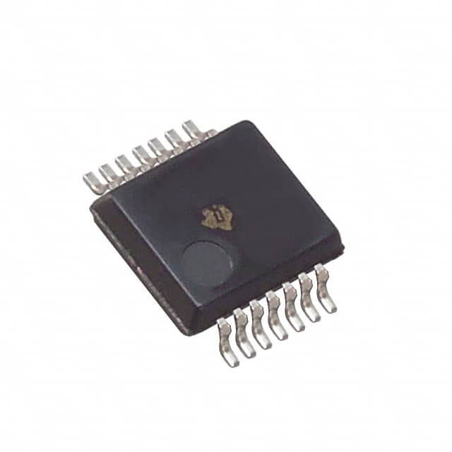
Lihat spesifikasi untuk detail produk.

SN74LS14DBR
Product Overview
- Category: Integrated Circuit (IC)
- Use: Logic Gate Inverter
- Characteristics: TTL (Transistor-Transistor Logic) technology, Hex Schmitt Trigger Inverter
- Package: SSOP (Shrink Small Outline Package)
- Essence: The SN74LS14DBR is a hex inverter gate IC that utilizes Schmitt trigger inputs to provide improved noise immunity and hysteresis characteristics.
- Packaging/Quantity: The SN74LS14DBR is available in tape and reel packaging with a quantity of 2500 units per reel.
Specifications
- Supply Voltage: 4.75V to 5.25V
- Input Voltage: 0V to Vcc
- Output Voltage: 0V to Vcc
- Operating Temperature Range: -40°C to +85°C
- Propagation Delay Time: 9ns (typical)
- Input Capacitance: 3pF (typical)
- Output Current: -0.4mA to 8mA
Detailed Pin Configuration
The SN74LS14DBR has a total of 14 pins arranged as follows:
- Pin 1: Input A1
- Pin 2: Output Y1
- Pin 3: Input A2
- Pin 4: Output Y2
- Pin 5: Input A3
- Pin 6: Output Y3
- Pin 7: Ground (GND)
- Pin 8: Output Y4
- Pin 9: Input A4
- Pin 10: Output Y5
- Pin 11: Input A5
- Pin 12: Output Y6
- Pin 13: Vcc (+5V)
- Pin 14: Input A6
Functional Features
- Hex Inverter Gates: The SN74LS14DBR consists of six independent inverter gates, each with a Schmitt trigger input.
- Improved Noise Immunity: The Schmitt trigger inputs provide improved noise immunity by adding hysteresis to the input signal, making the IC less sensitive to input voltage fluctuations.
- Hysteresis Characteristics: The hysteresis characteristics of the Schmitt trigger inputs ensure that the output transitions occur at different voltage levels for rising and falling input signals, reducing the possibility of false triggering.
Advantages and Disadvantages
Advantages
- Improved noise immunity due to Schmitt trigger inputs
- Hysteresis characteristics prevent false triggering
- Wide operating temperature range (-40°C to +85°C)
- Fast propagation delay time (9ns)
Disadvantages
- Limited supply voltage range (4.75V to 5.25V)
- Relatively low output current capability
Working Principles
The SN74LS14DBR operates as a hex inverter gate using TTL technology. Each inverter gate has a Schmitt trigger input, which provides hysteresis to the input signal. When the input voltage crosses a certain threshold level, the output switches state. The hysteresis ensures that the output transitions occur at different voltage levels for rising and falling input signals, improving noise immunity and preventing false triggering.
Detailed Application Field Plans
The SN74LS14DBR is commonly used in various digital logic applications, including:
- Signal Conditioning: The Schmitt trigger inputs make it suitable for conditioning noisy or weak input signals before further processing.
- Oscillators: The IC can be used to build relaxation oscillators or square wave generators.
- Level Shifting: It can be employed to shift logic levels between different voltage domains.
- Pulse Shaping: The hysteresis characteristics make it useful for shaping input pulses into well-defined output waveforms.
Detailed and Complete Alternative Models
Some alternative models to the SN74LS14DBR include:
- CD40106BE: Hex Schmitt Trigger Inverter IC from Texas Instruments
- MC14584B: Hex Schmitt Trigger Inverter IC from ON Semiconductor
- 74HC14: Hex Inverter with Schmitt Trigger Inputs IC from NXP Semiconductors
These alternative models offer similar functionality and can be used as replacements for the SN74LS14DBR in various applications.
Word count: 498 words
Sebutkan 10 pertanyaan dan jawaban umum terkait penerapan SN74LS14DBR dalam solusi teknis
Sure! Here are 10 common questions and answers related to the application of SN74LS14DBR:
Q: What is SN74LS14DBR? A: SN74LS14DBR is a hex inverter with Schmitt-trigger inputs, which means it can convert low-level signals to high-level signals and vice versa.
Q: What is the voltage supply range for SN74LS14DBR? A: The voltage supply range for SN74LS14DBR is typically between 4.75V and 5.25V.
Q: Can SN74LS14DBR be used with both CMOS and TTL logic levels? A: Yes, SN74LS14DBR is compatible with both CMOS and TTL logic levels.
Q: How many inverters are there in SN74LS14DBR? A: SN74LS14DBR has six inverters in a single package.
Q: What is the maximum operating frequency of SN74LS14DBR? A: The maximum operating frequency of SN74LS14DBR is typically around 20 MHz.
Q: Can SN74LS14DBR be used as a buffer? A: Yes, SN74LS14DBR can be used as a buffer to amplify or isolate signals.
Q: What is the input voltage range for SN74LS14DBR? A: The input voltage range for SN74LS14DBR is typically between 0V and Vcc (the supply voltage).
Q: Can SN74LS14DBR be used in high-speed applications? A: While SN74LS14DBR is not specifically designed for high-speed applications, it can still be used in moderate-speed applications.
Q: What is the output current capability of SN74LS14DBR? A: The output current capability of SN74LS14DBR is typically around 8 mA.
Q: Can SN74LS14DBR be used in automotive applications? A: Yes, SN74LS14DBR is suitable for use in automotive applications as it can operate within the required temperature range and withstand automotive voltage fluctuations.
Please note that these answers are general and may vary depending on specific datasheet specifications and application requirements.

