Lihat spesifikasi untuk detail produk.

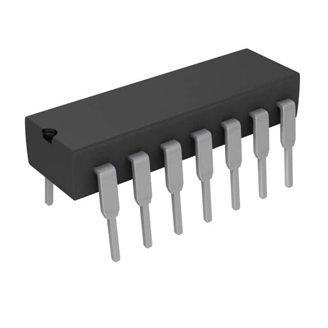
SN74LS02N
Product Overview
- Category: Integrated Circuit (IC)
- Use: Logic gate
- Characteristics: Quad 2-input NOR gate
- Package: DIP-14 (Dual In-line Package with 14 pins)
- Essence: Combines four NOR gates in a single package
- Packaging/Quantity: Available in tubes or reels, typically sold in quantities of 25 or more
Specifications
- Supply Voltage: 4.75V to 5.25V
- Input Voltage: 0V to Vcc
- Output Voltage: 0V to Vcc
- Operating Temperature Range: -40°C to +85°C
- Propagation Delay Time: 9ns (max)
- Power Dissipation: 22mW (typical)
Detailed Pin Configuration
The SN74LS02N has a total of 14 pins arranged as follows:
__    __
   1 |1  \__/ 14| Vcc
   2 |2        13| Output Y1
   3 |3        12| Input B1
   4 |4        11| Input A1
   5 |5        10| Output Y2
   6 |6         9| Input B2
   7 |7         8| Input A2
      |_________|
Functional Features
- Quad 2-input NOR gate: The SN74LS02N integrates four independent NOR gates into a single package.
- High-speed operation: With a propagation delay time of only 9ns, it allows for fast logic operations.
- Wide operating voltage range: It can operate within a supply voltage range of 4.75V to 5.25V.
- TTL compatibility: The SN74LS02N is compatible with TTL (Transistor-Transistor Logic) voltage levels.
Advantages and Disadvantages
Advantages: - Compact design: Combining four NOR gates in a single package saves space on the circuit board. - High-speed operation: The low propagation delay time enables quick logic operations. - Versatile: Can be used in various digital logic applications.
Disadvantages: - Limited functionality: Only performs NOR gate operations, limiting its use to specific logic functions. - Power consumption: Consumes power even when not actively switching.
Working Principles
The SN74LS02N operates based on the principles of Boolean logic. It takes two input signals and produces an output signal based on the NOR gate truth table. When both inputs are low (0), the output is high (1). In all other cases, the output is low (0).
Detailed Application Field Plans
The SN74LS02N can be used in various digital logic applications, including:
- Data processing systems
- Arithmetic circuits
- Control systems
- Memory address decoding
- Clock synchronization circuits
- Signal conditioning circuits
Detailed and Complete Alternative Models
Some alternative models that provide similar functionality to the SN74LS02N include:
- 74HC02: Quad 2-input NOR gate with CMOS technology.
- CD4001: Quad 2-input NOR gate with CMOS technology.
- MC14093B: Quad 2-input NAND gate with CMOS technology.
These alternatives offer similar logic gate functionality but may have different characteristics, specifications, or package types.
Word count: 378 words
Sebutkan 10 pertanyaan dan jawaban umum terkait penerapan SN74LS02N dalam solusi teknis
Sure! Here are 10 common questions and answers related to the application of SN74LS02N in technical solutions:
Question: What is SN74LS02N?
- Answer: SN74LS02N is a quad 2-input NOR gate integrated circuit (IC) that is commonly used in digital logic circuits.Question: What is the purpose of using SN74LS02N in technical solutions?
- Answer: SN74LS02N is used to perform logical NOR operations in various digital applications, such as signal processing, data manipulation, and control systems.Question: How many inputs does SN74LS02N have?
- Answer: SN74LS02N has four independent 2-input NOR gates, which means it can handle up to eight input signals.Question: What is the voltage range supported by SN74LS02N?
- Answer: SN74LS02N operates with a supply voltage range of 4.75V to 5.25V.Question: What is the maximum current output of SN74LS02N?
- Answer: The maximum current output per gate of SN74LS02N is typically around 8mA.Question: Can SN74LS02N be used for both TTL and CMOS logic levels?
- Answer: Yes, SN74LS02N is compatible with both TTL (Transistor-Transistor Logic) and CMOS (Complementary Metal-Oxide-Semiconductor) logic levels.Question: What is the operating temperature range of SN74LS02N?
- Answer: SN74LS02N can operate within a temperature range of -40°C to 85°C.Question: Is SN74LS02N suitable for high-speed applications?
- Answer: SN74LS02N is not specifically designed for high-speed applications. It is more commonly used in medium-speed digital circuits.Question: Can I cascade multiple SN74LS02N ICs together?
- Answer: Yes, you can cascade multiple SN74LS02N ICs to increase the number of NOR gates or inputs in your circuit.Question: Are there any alternative ICs that can be used instead of SN74LS02N?
- Answer: Yes, there are alternative ICs available, such as 74HC02 or CD4001, which also provide quad 2-input NOR gates and may have different specifications or features.
Please note that the answers provided here are general and may vary depending on specific datasheets and application requirements.

