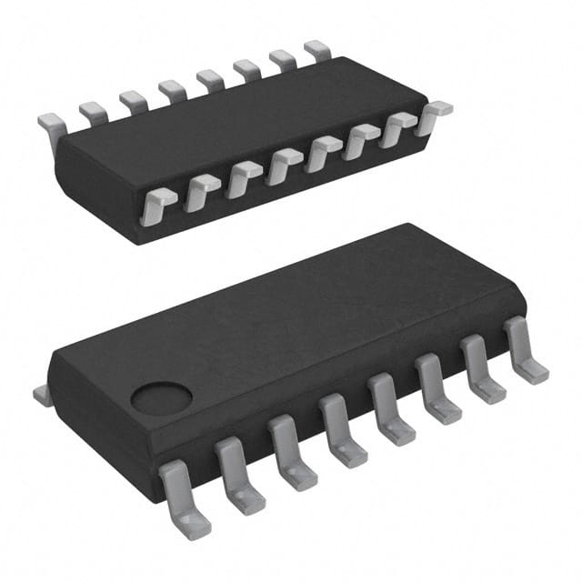
Lihat spesifikasi untuk detail produk.

SN74HC367DR
Product Overview
- Category: Integrated Circuit (IC)
- Use: Buffer/Line Driver
- Characteristics: High-speed, Non-Inverting, Tri-State
- Package: SOIC (Small Outline Integrated Circuit)
- Essence: Hex Bus Buffer with 3-State Outputs
- Packaging/Quantity: Tape and Reel, 2500 pieces per reel
Specifications
- Supply Voltage Range: 2V to 6V
- High-Level Input Voltage: 2V to VCC
- Low-Level Input Voltage: GND to 0.8V
- High-Level Output Voltage: VCC - 0.5V
- Low-Level Output Voltage: 0.5V
- Maximum Operating Frequency: 80MHz
- Propagation Delay Time: 9ns
- Output Current: ±6mA
Detailed Pin Configuration
The SN74HC367DR has a total of 16 pins arranged as follows:
- OE (Output Enable) 1
- A1 (Input A1)
- Y1 (Output Y1)
- A2 (Input A2)
- Y2 (Output Y2)
- A3 (Input A3)
- Y3 (Output Y3)
- GND (Ground)
- Y4 (Output Y4)
- A4 (Input A4)
- Y5 (Output Y5)
- A5 (Input A5)
- Y6 (Output Y6)
- VCC (Supply Voltage)
- OE (Output Enable) 2
- GND (Ground)
Functional Features
- Hex buffer with 3-state outputs
- Non-inverting logic
- High-speed operation
- Wide supply voltage range
- Output enable control for tri-state operation
Advantages and Disadvantages
Advantages: - High-speed operation allows for efficient data transfer - Non-inverting logic simplifies circuit design - Wide supply voltage range provides flexibility in various applications - Tri-state outputs enable bus sharing and reduce conflicts
Disadvantages: - Limited output current may restrict use in certain high-power applications - Propagation delay time may affect timing-sensitive systems
Working Principles
The SN74HC367DR is a hex buffer with 3-state outputs. It operates by receiving input signals on the A1 to A6 pins and providing non-inverted outputs on the Y1 to Y6 pins. The output enable (OE) pins control the tri-state operation, allowing the outputs to be either active or in a high-impedance state.
Detailed Application Field Plans
The SN74HC367DR is commonly used in various applications, including:
- Data communication systems
- Address decoding circuits
- Memory interfacing
- Bus drivers
- Clock distribution networks
Detailed and Complete Alternative Models
Some alternative models that can be considered as alternatives to the SN74HC367DR are:
- SN74HC365DR: Hex Buffer/Driver with 3-State Outputs
- SN74HC368DR: Hex Bus Driver with 3-State Outputs
- SN74HC366DR: Hex Buffer/Line Driver with 3-State Outputs
- SN74HC364DR: Hex Inverter/Buffer with 3-State Outputs
These alternative models offer similar functionality and characteristics, providing options for different design requirements.
Word count: 399 words
Sebutkan 10 pertanyaan dan jawaban umum terkait penerapan SN74HC367DR dalam solusi teknis
Sure! Here are 10 common questions and answers related to the application of SN74HC367DR in technical solutions:
Question: What is SN74HC367DR?
- Answer: SN74HC367DR is a high-speed hex bus driver with three-state outputs, commonly used in digital logic applications.Question: What is the voltage supply range for SN74HC367DR?
- Answer: The voltage supply range for SN74HC367DR is typically between 2V and 6V.Question: How many output pins does SN74HC367DR have?
- Answer: SN74HC367DR has six output pins, each with a three-state capability.Question: Can SN74HC367DR be used as a level shifter?
- Answer: Yes, SN74HC367DR can be used as a level shifter to convert signals between different voltage levels.Question: What is the maximum operating frequency of SN74HC367DR?
- Answer: The maximum operating frequency of SN74HC367DR is typically around 50 MHz.Question: Can SN74HC367DR drive LEDs directly?
- Answer: Yes, SN74HC367DR can drive LEDs directly by connecting them to the output pins through appropriate current-limiting resistors.Question: Is SN74HC367DR compatible with TTL logic levels?
- Answer: Yes, SN74HC367DR is compatible with TTL logic levels, making it suitable for interfacing with TTL devices.Question: Can SN74HC367DR be used in bidirectional data transfer applications?
- Answer: No, SN74HC367DR is a unidirectional bus driver and cannot be used for bidirectional data transfer.Question: What is the output current capability of SN74HC367DR?
- Answer: The output current capability of SN74HC367DR is typically around 8 mA.Question: Can SN74HC367DR be used in automotive applications?
- Answer: Yes, SN74HC367DR is suitable for use in automotive applications as it can operate within the required temperature range and voltage levels.
Please note that these answers are general and may vary depending on specific application requirements and datasheet specifications.

