

Lihat spesifikasi untuk detail produk.
SN74GTLP817DGVRG4
Product Overview
- Category: Integrated Circuit
- Use: Signal Level Translator
- Characteristics: High-speed, low-voltage, low-power consumption
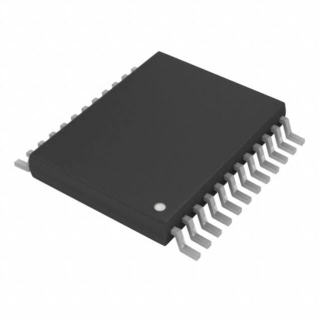
- Package: VSSOP (Very Small Outline Package)
- Essence: Translates signals between different voltage levels
- Packaging/Quantity: Tape and Reel, 2500 units per reel
Specifications
- Supply Voltage Range: 1.2V to 3.6V
- Input Voltage Range: 0V to VCCA + 0.5V
- Output Voltage Range: 0V to VCCB + 0.5V
- Operating Temperature Range: -40°C to +85°C
- Maximum Data Rate: 400 Mbps
Detailed Pin Configuration
The SN74GTLP817DGVRG4 has a total of 16 pins:
- VCCA: Power supply for the A-side logic
- GND: Ground reference for the A-side logic
- A1: Input or output pin for the A-side logic
- A2: Input or output pin for the A-side logic
- A3: Input or output pin for the A-side logic
- A4: Input or output pin for the A-side logic
- VCCB: Power supply for the B-side logic
- GND: Ground reference for the B-side logic
- B1: Input or output pin for the B-side logic
- B2: Input or output pin for the B-side logic
- B3: Input or output pin for the B-side logic
- B4: Input or output pin for the B-side logic
- OE: Output enable pin
- SEL: Select pin
- GND: Ground reference for the device
- VCC: Power supply for the device
Functional Features
- Bidirectional voltage level translation
- Supports multiple voltage domains
- High-speed data transmission
- Low power consumption
- ESD protection on all pins
- Output enable and select control options
Advantages and Disadvantages
Advantages: - Wide supply voltage range - High-speed data rate - Small package size - ESD protection on all pins
Disadvantages: - Limited number of I/O pins - Not suitable for high-power applications
Working Principles
The SN74GTLP817DGVRG4 is designed to translate signals between different voltage levels. It uses a combination of level shifters and voltage dividers to ensure proper signal translation. The device operates bidirectionally, allowing signals to be translated from one voltage domain to another.
Detailed Application Field Plans
The SN74GTLP817DGVRG4 can be used in various applications, including:
- Communication systems
- Data transmission interfaces
- Industrial automation
- Consumer electronics
- Automotive electronics
Detailed and Complete Alternative Models
Some alternative models that offer similar functionality to the SN74GTLP817DGVRG4 are:
- SN74LVC1T45DBVR
- SN74AVC4T245RGYR
- SN74LVC8T245PW
These models provide voltage level translation capabilities and are available in different package options.
In conclusion, the SN74GTLP817DGVRG4 is a versatile integrated circuit that enables efficient signal level translation between different voltage domains. Its high-speed operation, low power consumption, and small package size make it suitable for a wide range of applications in various industries.
Sebutkan 10 pertanyaan dan jawaban umum terkait penerapan SN74GTLP817DGVRG4 dalam solusi teknis
Sure! Here are 10 common questions and answers related to the application of SN74GTLP817DGVRG4 in technical solutions:
Q: What is SN74GTLP817DGVRG4? A: SN74GTLP817DGVRG4 is a high-speed, low-power voltage level translator IC designed for use in various technical solutions.
Q: What is the voltage range supported by SN74GTLP817DGVRG4? A: SN74GTLP817DGVRG4 supports voltage translation from 1.2V to 3.3V on the low side and 1.8V to 5.5V on the high side.
Q: Can SN74GTLP817DGVRG4 be used bidirectionally? A: Yes, SN74GTLP817DGVRG4 can perform bidirectional voltage translation between the low and high sides.
Q: What is the maximum data rate supported by SN74GTLP817DGVRG4? A: SN74GTLP817DGVRG4 supports data rates up to 200 Mbps.
Q: Is SN74GTLP817DGVRG4 suitable for I2C or SPI interfaces? A: Yes, SN74GTLP817DGVRG4 can be used for voltage level translation in I2C, SPI, and other similar serial communication interfaces.
Q: Does SN74GTLP817DGVRG4 require external power supply decoupling capacitors? A: Yes, it is recommended to use external power supply decoupling capacitors for optimal performance of SN74GTLP817DGVRG4.
Q: Can SN74GTLP817DGVRG4 tolerate overvoltage conditions? A: SN74GTLP817DGVRG4 has built-in protection features to tolerate overvoltage conditions on the high side.
Q: What is the operating temperature range of SN74GTLP817DGVRG4? A: SN74GTLP817DGVRG4 can operate within a temperature range of -40°C to 85°C.
Q: Can SN74GTLP817DGVRG4 be used in automotive applications? A: Yes, SN74GTLP817DGVRG4 is qualified for automotive applications and meets the necessary standards.
Q: Are there any evaluation boards or reference designs available for SN74GTLP817DGVRG4? A: Yes, Texas Instruments provides evaluation boards and reference designs that can help in understanding and implementing SN74GTLP817DGVRG4 in various technical solutions.
Please note that these answers are general and may vary depending on specific application requirements. It is always recommended to refer to the datasheet and application notes provided by the manufacturer for detailed information.