

Lihat spesifikasi untuk detail produk.
SN74FB2040RCRG3
Product Overview
- Category: Integrated Circuit (IC)
- Use: Logic Gate
- Characteristics: High-speed, low-power consumption
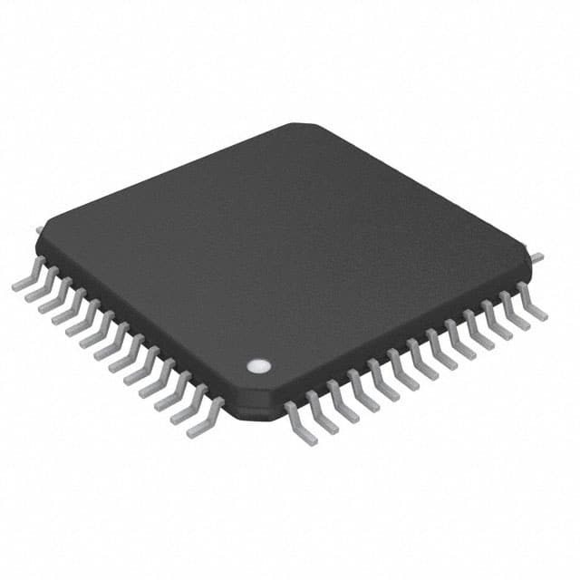
- Package: QFN (Quad Flat No-leads)
- Essence: Digital logic gate with multiple inputs and outputs
- Packaging/Quantity: Tape and Reel, 2500 units per reel
Specifications
- Supply Voltage: 1.65V to 3.6V
- Input Voltage: 0V to VCC
- Output Voltage: 0V to VCC
- Operating Temperature Range: -40°C to +85°C
- Propagation Delay: 2.5ns (typical)
- Maximum Frequency: 400MHz
Detailed Pin Configuration
The SN74FB2040RCRG3 has a total of 20 pins arranged as follows:
- A1
- B1
- C1
- D1
- E1
- F1
- G1
- H1
- Y1
- Y2
- Y3
- Y4
- Y5
- Y6
- Y7
- Y8
- Y9
- Y10
- GND
- VCC
Functional Features
- Multiple input AND/OR gates
- High-speed operation
- Low power consumption
- Schmitt-trigger inputs for noise immunity
- Wide operating voltage range
- 3-state outputs for bus-oriented applications
Advantages and Disadvantages
Advantages: - High-speed operation allows for efficient data processing - Low power consumption reduces energy usage - Schmitt-trigger inputs provide noise immunity, ensuring reliable operation - Wide operating voltage range allows for compatibility with various systems - 3-state outputs enable bus-oriented applications
Disadvantages: - Limited number of inputs and outputs - Not suitable for complex logic operations requiring more inputs
Working Principles
The SN74FB2040RCRG3 is a digital logic gate that performs multiple input AND/OR operations. It operates by receiving input signals through its various input pins (A1 to H1) and producing the corresponding output signals (Y1 to Y10). The gate utilizes advanced semiconductor technology to achieve high-speed operation and low power consumption.
Detailed Application Field Plans
The SN74FB2040RCRG3 is commonly used in various digital systems, including:
- Microprocessors and microcontrollers
- Communication systems
- Data storage devices
- Industrial automation
- Automotive electronics
In microprocessors and microcontrollers, the gate is utilized for data processing and control functions. In communication systems, it helps in signal routing and protocol handling. Data storage devices employ the gate for address decoding and data manipulation. Industrial automation relies on the gate for control and monitoring tasks. Automotive electronics utilize the gate for various applications, such as engine management and safety systems.
Detailed and Complete Alternative Models
- SN74FB2040RCR: Similar specifications and features, but available in a different package (SOIC).
- SN74FB2040RCRGR: Similar specifications and features, but available in a different package (VQFN).
- SN74FB2040RCRG4: Upgraded version with improved performance and additional features.
These alternative models provide similar functionality to the SN74FB2040RCRG3 but may differ in package type or offer enhanced capabilities.
Word count: 386 words
Sebutkan 10 pertanyaan dan jawaban umum terkait penerapan SN74FB2040RCRG3 dalam solusi teknis
Sure! Here are 10 common questions and answers related to the application of SN74FB2040RCRG3 in technical solutions:
Q: What is SN74FB2040RCRG3? A: SN74FB2040RCRG3 is a specific model of integrated circuit (IC) manufactured by Texas Instruments.
Q: What is the purpose of SN74FB2040RCRG3? A: SN74FB2040RCRG3 is a high-speed, low-power buffer and level translator IC designed for use in various digital communication systems.
Q: What voltage levels does SN74FB2040RCRG3 support? A: SN74FB2040RCRG3 supports voltage translation between 1.2V and 3.6V.
Q: Can SN74FB2040RCRG3 be used for bidirectional voltage translation? A: Yes, SN74FB2040RCRG3 supports bidirectional voltage translation, making it suitable for applications where data needs to be translated in both directions.
Q: What is the maximum data rate supported by SN74FB2040RCRG3? A: SN74FB2040RCRG3 can support data rates up to 100 Mbps.
Q: Is SN74FB2040RCRG3 compatible with different logic families? A: Yes, SN74FB2040RCRG3 is compatible with various logic families such as TTL, CMOS, and LVCMOS.
Q: Can SN74FB2040RCRG3 be used in automotive applications? A: Yes, SN74FB2040RCRG3 is qualified for automotive applications and meets the necessary standards.
Q: Does SN74FB2040RCRG3 have built-in ESD protection? A: Yes, SN74FB2040RCRG3 has built-in ESD protection to safeguard against electrostatic discharge.
Q: What is the operating temperature range of SN74FB2040RCRG3? A: SN74FB2040RCRG3 can operate within a temperature range of -40°C to +125°C.
Q: Are there any application examples for SN74FB2040RCRG3? A: Yes, SN74FB2040RCRG3 can be used in various applications such as level shifting in communication interfaces, voltage translation between different logic levels, and interfacing microcontrollers with different peripherals.
Please note that these answers are general and may vary depending on specific use cases and requirements.