Lihat spesifikasi untuk detail produk.

SN74F138NSR
Product Overview
Category
SN74F138NSR belongs to the category of integrated circuits (ICs).
Use
This product is commonly used in digital logic applications, specifically for decoding purposes.
Characteristics
- High-speed operation
- Low power consumption
- Wide operating voltage range
- Multiple output enable inputs
- Compact size
Package
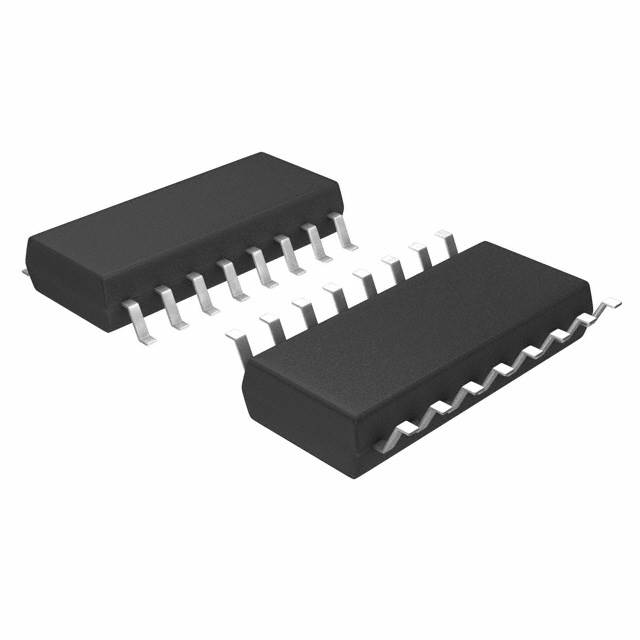
SN74F138NSR is available in a small-outline package (SOIC) with 16 pins.
Essence
The essence of SN74F138NSR lies in its ability to decode binary information and select one of the multiple outputs based on the input signals.
Packaging/Quantity
This product is typically packaged in reels or tubes, with each containing a specific quantity of ICs. The exact quantity may vary depending on the manufacturer's specifications.
Specifications
- Supply Voltage: 2V - 6V
- Operating Temperature Range: -40°C to +85°C
- Output Current: ±4mA
- Propagation Delay Time: 10ns (max)
- Input Capacitance: 3pF (typ)
Detailed Pin Configuration
- GND (Ground)
- A0 (Address Input 0)
- A1 (Address Input 1)
- A2 (Address Input 2)
- E1 (Enable Input 1)
- E2 (Enable Input 2)
- Y0 (Output 0)
- Y1 (Output 1)
- Y2 (Output 2)
- Y3 (Output 3)
- VCC (Supply Voltage)
- Y4 (Output 4)
- Y5 (Output 5)
- Y6 (Output 6)
- Y7 (Output 7)
- VCC (Supply Voltage)
Functional Features
- Decodes 3-bit binary information into 8 output lines
- Multiple enable inputs for flexible control
- High-speed operation allows for efficient data processing
- Low power consumption ensures energy efficiency
Advantages and Disadvantages
Advantages
- Compact size makes it suitable for space-constrained applications
- Wide operating voltage range enables compatibility with various systems
- High-speed operation facilitates quick data decoding
- Low power consumption helps conserve energy
Disadvantages
- Limited number of address inputs restricts the range of input combinations
- Propagation delay time may affect real-time applications
Working Principles
SN74F138NSR operates based on the principle of binary decoding. It takes a 3-bit binary input and decodes it into one of the eight possible output lines. The enable inputs (E1 and E2) control the activation of the outputs, allowing for selective output based on the input combination.
Detailed Application Field Plans
SN74F138NSR finds application in various digital systems, including but not limited to: - Address decoding in microcontrollers and microprocessors - Memory selection in RAM modules - Data routing in multiplexers - Signal demultiplexing in communication systems
Detailed and Complete Alternative Models
Some alternative models that serve similar functions to SN74F138NSR include: - 74HC138: A CMOS version with similar pin configuration and functionality - CD74HCT138: A high-speed TTL version with comparable characteristics - DM74LS138: A low-power Schottky version with compatible pinout
These alternatives can be considered based on specific requirements and system compatibility.
Word count: 526 words
Sebutkan 10 pertanyaan dan jawaban umum terkait penerapan SN74F138NSR dalam solusi teknis
Sure! Here are 10 common questions and answers related to the application of SN74F138NSR in technical solutions:
Question: What is SN74F138NSR?
Answer: SN74F138NSR is a 3-to-8 line decoder/demultiplexer integrated circuit (IC) manufactured by Texas Instruments.Question: What is the purpose of SN74F138NSR?
Answer: SN74F138NSR is used to decode binary information from a digital input and activate one of the eight outputs based on the input combination.Question: What is the maximum operating voltage for SN74F138NSR?
Answer: The maximum operating voltage for SN74F138NSR is 5.5 volts.Question: How many inputs does SN74F138NSR have?
Answer: SN74F138NSR has three inputs: A0, A1, and A2.Question: How many outputs does SN74F138NSR have?
Answer: SN74F138NSR has eight outputs: Y0, Y1, Y2, Y3, Y4, Y5, Y6, and Y7.Question: What is the output logic level of SN74F138NSR?
Answer: The output logic level of SN74F138NSR is TTL-compatible.Question: Can SN74F138NSR be cascaded to increase the number of decoded outputs?
Answer: Yes, multiple SN74F138NSR ICs can be cascaded together to increase the number of decoded outputs.Question: What is the typical propagation delay of SN74F138NSR?
Answer: The typical propagation delay of SN74F138NSR is 10 nanoseconds.Question: Can SN74F138NSR be used in both active-high and active-low applications?
Answer: Yes, SN74F138NSR can be used in both active-high and active-low applications by appropriately connecting the enable (E) pin.Question: What is the package type of SN74F138NSR?
Answer: SN74F138NSR is available in a small-outline integrated circuit (SOIC) package.
Please note that these answers are general and may vary depending on specific datasheet specifications and application requirements.

