

Lihat spesifikasi untuk detail produk.
SN74CBTD16211DGVR
Product Overview
- Category: Integrated Circuit
- Use: Digital Multiplexer/Demultiplexer
- Characteristics:
- High-speed switching capability
- Low power consumption
- Wide operating voltage range
- Small package size
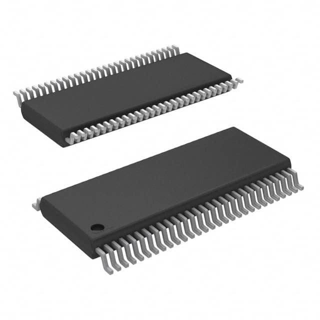
- Package: VSSOP (Very Small Outline Package)
- Essence: This integrated circuit is designed to provide digital multiplexing and demultiplexing functionality in various electronic systems.
- Packaging/Quantity: Available in reels, with a quantity of 3000 units per reel.
Specifications
- Number of Channels: 24
- Input Voltage Range: 0V to VCC
- Output Voltage Range: 0V to VCC
- Operating Voltage Range: 1.65V to 3.6V
- Maximum Propagation Delay Time: 2.5ns
- Maximum Operating Frequency: 400MHz
- Operating Temperature Range: -40°C to +85°C
Detailed Pin Configuration
The SN74CBTD16211DGVR has a total of 56 pins, which are organized as follows:
- Pin 1: GND (Ground)
- Pin 2: A0 (Multiplexer Address Input)
- Pin 3: A1 (Multiplexer Address Input)
- Pin 4: A2 (Multiplexer Address Input)
- ...
- Pin 55: Y23 (Demultiplexer Output)
- Pin 56: VCC (Power Supply)
Functional Features
- Digital Multiplexing: The SN74CBTD16211DGVR can select one of the 24 input channels and route it to the output based on the address inputs.
- Digital Demultiplexing: It can take a single input and distribute it to one of the 24 output channels based on the address inputs.
- High-Speed Switching: The integrated circuit can switch between channels with minimal delay, making it suitable for applications requiring fast data routing.
- Low Power Consumption: The SN74CBTD16211DGVR is designed to operate efficiently, minimizing power consumption in electronic systems.
- Wide Operating Voltage Range: It can operate within a voltage range of 1.65V to 3.6V, providing flexibility in various applications.
Advantages and Disadvantages
Advantages: - High-speed switching capability enables efficient data routing. - Low power consumption helps conserve energy in electronic systems. - Wide operating voltage range allows compatibility with different power supply levels. - Small package size saves board space in compact designs.
Disadvantages: - Limited number of channels (24) may not be sufficient for certain applications requiring more inputs/outputs. - Propagation delay time (2.5ns) may introduce latency in time-critical applications.
Working Principles
The SN74CBTD16211DGVR operates based on the principles of digital multiplexing and demultiplexing. It uses the address inputs (A0, A1, A2) to select the desired input channel and route it to the output pin (Y23). The integrated circuit utilizes internal logic gates and switches to achieve this functionality.
Detailed Application Field Plans
The SN74CBTD16211DGVR finds applications in various electronic systems, including but not limited to: - Data communication equipment - Networking devices - Test and measurement instruments - Industrial automation systems - Consumer electronics
Detailed and Complete Alternative Models
- SN74CBTD3306CPW: 8-channel digital multiplexer/demultiplexer with similar characteristics and package.
- SN74CBT3257DGV: 4-channel digital multiplexer/demultiplexer with enhanced ESD protection and small package size.
- SN74CBT16212ADGGR: 24-channel digital multiplexer/demultiplexer with higher operating frequency and lower propagation delay.
These alternative models offer similar functionality to the SN74CBTD16211DGVR but may have different specifications or additional features based on specific application requirements.
Word count: 408 words
Sebutkan 10 pertanyaan dan jawaban umum terkait penerapan SN74CBTD16211DGVR dalam solusi teknis
Sure! Here are 10 common questions and answers related to the application of SN74CBTD16211DGVR:
Q: What is SN74CBTD16211DGVR? A: SN74CBTD16211DGVR is a high-performance, 24-bit bus switch with 5V tolerant inputs and outputs.
Q: What is the purpose of SN74CBTD16211DGVR? A: SN74CBTD16211DGVR is used to enable or disable the connection between two buses, allowing for bidirectional data flow.
Q: What voltage levels does SN74CBTD16211DGVR support? A: SN74CBTD16211DGVR supports both 3.3V and 5V voltage levels.
Q: How many channels does SN74CBTD16211DGVR have? A: SN74CBTD16211DGVR has 24 channels, allowing for the switching of up to 24 signals.
Q: Can SN74CBTD16211DGVR handle high-speed data signals? A: Yes, SN74CBTD16211DGVR is designed to handle high-speed data signals, making it suitable for various applications.
Q: What is the maximum current rating of SN74CBTD16211DGVR? A: The maximum current rating of SN74CBTD16211DGVR is typically around 32mA per channel.
Q: Is SN74CBTD16211DGVR compatible with different logic families? A: Yes, SN74CBTD16211DGVR is compatible with various logic families such as TTL, CMOS, and LVCMOS.
Q: Can SN74CBTD16211DGVR be used in hot-swapping applications? A: Yes, SN74CBTD16211DGVR supports hot-swapping, allowing for the connection and disconnection of devices without power interruption.
Q: What is the operating temperature range of SN74CBTD16211DGVR? A: SN74CBTD16211DGVR can operate within a temperature range of -40°C to 85°C.
Q: Are there any specific application examples for SN74CBTD16211DGVR? A: SN74CBTD16211DGVR can be used in various applications such as data acquisition systems, industrial automation, and communication equipment.
Please note that these answers are general and may vary depending on the specific requirements and conditions of your technical solution.