

Lihat spesifikasi untuk detail produk.
SN74CB3T3253DGVR
Product Overview
- Category: Integrated Circuit (IC)
- Use: Multiplexer/Demultiplexer
- Characteristics:
- Low voltage operation
- High-speed switching
- Wide operating temperature range
- Small package size
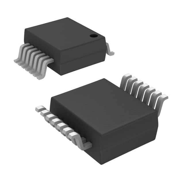
- Package: VSSOP (Very Small Outline Package)
- Essence: This IC is a multiplexer/demultiplexer that allows for the selection of one of two input signals to be routed to an output line.
- Packaging/Quantity: Available in tape and reel packaging, with 3000 units per reel.
Specifications
- Supply Voltage Range: 1.65V to 3.6V
- Input Voltage Range: 0V to VCC
- Output Voltage Range: 0V to VCC
- Operating Temperature Range: -40°C to +85°C
- On-state Resistance: 4Ω (typical)
- Bandwidth: 400MHz (typical)
Detailed Pin Configuration
The SN74CB3T3253DGVR has a total of 16 pins, which are assigned as follows:
- A0: Address input bit 0
- A1: Address input bit 1
- OE: Output enable
- S: Select input
- I0: Data input 0
- I1: Data input 1
- Y: Output
- GND: Ground
- NC: No connection
- B0: Address input bit 0
- B1: Address input bit 1
- OE: Output enable
- S: Select input
- I0: Data input 0
- I1: Data input 1
- VCC: Power supply
Functional Features
- Dual 2-channel multiplexer/demultiplexer
- Low power consumption
- Wide operating voltage range
- Fast switching speed
- Break-before-make switching action
Advantages and Disadvantages
Advantages: - Small package size allows for space-saving designs - Wide operating temperature range enables usage in various environments - Low voltage operation reduces power consumption - High-speed switching ensures efficient signal routing
Disadvantages: - Limited number of input/output channels (2 channels) - Relatively high on-state resistance may introduce signal attenuation
Working Principles
The SN74CB3T3253DGVR operates as a multiplexer/demultiplexer by utilizing address inputs (A0, A1) to select one of the two data inputs (I0, I1) and route it to the output pin (Y). The select input (S) determines whether the IC functions as a multiplexer or demultiplexer. When S is low, the IC acts as a multiplexer, and when S is high, it functions as a demultiplexer.
Detailed Application Field Plans
The SN74CB3T3253DGVR can be used in various applications, including:
- Data communication systems: It can be employed to switch between different data sources or destinations.
- Audio/video equipment: The IC can be utilized to select audio or video signals from multiple sources and route them to the appropriate output devices.
- Test and measurement instruments: It can be integrated into test setups to switch between different test points or instruments.
- Industrial control systems: The IC can be used for signal routing in control systems, allowing for flexible configuration.
Detailed and Complete Alternative Models
- CD74HC4052E: This IC is a similar 2-channel analog multiplexer/demultiplexer with a DIP package.
- SN74LVC2G157DCTR: A 2-channel multiplexer/demultiplexer with a smaller package size and lower on-state resistance.
- CD4051BE: A 1-channel analog multiplexer/demultiplexer with a DIP package.
These alternative models offer similar functionality to the SN74CB3T3253DGVR and can be considered based on specific requirements and design constraints.
Word count: 536 words
Sebutkan 10 pertanyaan dan jawaban umum terkait penerapan SN74CB3T3253DGVR dalam solusi teknis
Sure! Here are 10 common questions and answers related to the application of SN74CB3T3253DGVR in technical solutions:
Q: What is SN74CB3T3253DGVR? A: SN74CB3T3253DGVR is a multiplexer/demultiplexer IC (Integrated Circuit) that allows for bidirectional level translation between different voltage domains.
Q: What are the key features of SN74CB3T3253DGVR? A: Some key features include low ON-state resistance, wide voltage range support, low power consumption, and compatibility with various logic families.
Q: How can SN74CB3T3253DGVR be used in technical solutions? A: It can be used to interface between devices operating at different voltage levels, such as microcontrollers, sensors, and communication modules.
Q: What is the voltage range supported by SN74CB3T3253DGVR? A: SN74CB3T3253DGVR supports a voltage range from 1.2V to 5.5V, making it compatible with many common voltage levels.
Q: Can SN74CB3T3253DGVR handle bidirectional communication? A: Yes, SN74CB3T3253DGVR is designed to support bidirectional data flow, allowing for both input and output signals.
Q: How many channels does SN74CB3T3253DGVR have? A: SN74CB3T3253DGVR has two independent channels, which can be used to connect two different voltage domains.
Q: What is the maximum data rate supported by SN74CB3T3253DGVR? A: SN74CB3T3253DGVR can handle data rates up to 100 Mbps, making it suitable for many high-speed communication applications.
Q: Does SN74CB3T3253DGVR have any built-in protection features? A: Yes, SN74CB3T3253DGVR has built-in ESD (Electrostatic Discharge) protection, which helps safeguard against voltage spikes and transients.
Q: Can SN74CB3T3253DGVR be used in battery-powered applications? A: Yes, SN74CB3T3253DGVR has low power consumption and can be used in battery-powered devices without significantly draining the battery.
Q: Are there any recommended application circuits or reference designs available for SN74CB3T3253DGVR? A: Yes, Texas Instruments provides application notes and reference designs that showcase different use cases and circuit configurations for SN74CB3T3253DGVR.
Please note that these answers are general and may vary depending on specific design requirements and application scenarios.