

Lihat spesifikasi untuk detail produk.
SN74AUP3G17YFPR
Product Overview
- Category: Integrated Circuit (IC)
- Use: Logic Gate
- Characteristics: High-speed, Low-power, Triple Schmitt-Trigger Buffer/Inverter
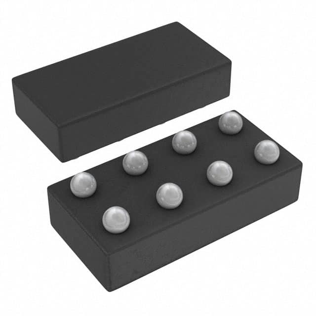
- Package: 6-Bump DSBGA (0.8mm x 1.2mm)
- Essence: This IC is designed to provide buffering and inverting functionality for digital signals in various electronic circuits.
- Packaging/Quantity: Tape and Reel, 3000 units per reel
Specifications
- Supply Voltage Range: 0.8V to 3.6V
- Input Voltage Range: 0V to VCC
- Output Voltage Range: 0V to VCC
- Operating Temperature Range: -40°C to +85°C
- Propagation Delay: 2.5ns (typical)
- Output Drive Capability: ±24mA
- Input Capacitance: 1.5pF (typical)
Detailed Pin Configuration
The SN74AUP3G17YFPR has a total of 6 pins:
- Pin 1: Input A
- Pin 2: Output Y
- Pin 3: Ground (GND)
- Pin 4: Power Supply (VCC)
- Pin 5: Input B
- Pin 6: Input C
Functional Features
- Triple Schmitt-Trigger Buffer/Inverter with independent inputs (A, B, C)
- High-speed operation suitable for use in high-frequency applications
- Low-power consumption, making it ideal for battery-powered devices
- Wide supply voltage range allows compatibility with various systems
- Robust design with high output drive capability
Advantages and Disadvantages
Advantages
- High-speed operation enables efficient signal processing
- Low-power consumption extends battery life in portable devices
- Wide supply voltage range provides flexibility in system integration
- Small package size saves board space in compact designs
- Robust output drive capability ensures reliable signal transmission
Disadvantages
- Limited number of inputs and outputs restricts complex circuit configurations
- Not suitable for applications requiring high noise immunity
Working Principles
The SN74AUP3G17YFPR is based on Schmitt-trigger logic, which utilizes positive feedback to provide hysteresis and improve noise immunity. It accepts digital input signals and buffers or inverts them based on the logic level applied to the inputs. The output follows the input with a slight delay due to propagation delay.
Detailed Application Field Plans
The SN74AUP3G17YFPR can be used in various electronic circuits that require buffering or inversion of digital signals. Some potential application fields include:
- Communication Systems: Signal conditioning and level shifting in data transmission circuits.
- Consumer Electronics: Interface between microcontrollers and peripheral devices.
- Automotive Electronics: Signal processing in automotive control units.
- Industrial Automation: Logic level conversion in PLCs and industrial control systems.
- Medical Devices: Signal conditioning in medical monitoring equipment.
Detailed and Complete Alternative Models
- SN74AUP1G17DBVR: Single Schmitt-Trigger Buffer/Inverter, SOT-23 package.
- SN74LVC3G17DCUR: Triple Schmitt-Trigger Buffer/Inverter, USON-6 package.
- SN74HCT17N: Hex Schmitt-Trigger Inverter, DIP-14 package.
- SN74LV1T34DCKR: Single Schmitt-Trigger Buffer, SC-70 package.
- SN74AHC1G14DBVR: Single Schmitt-Trigger Inverter, SOT-23 package.
(Note: This is not an exhaustive list. Please refer to the manufacturer's datasheets for a complete list of alternative models.)
Word count: 445 words
Sebutkan 10 pertanyaan dan jawaban umum terkait penerapan SN74AUP3G17YFPR dalam solusi teknis
Sure! Here are 10 common questions and answers related to the application of SN74AUP3G17YFPR in technical solutions:
Q: What is SN74AUP3G17YFPR? A: SN74AUP3G17YFPR is a triple Schmitt-trigger buffer with open-drain outputs, commonly used in digital logic circuits.
Q: What is the voltage supply range for SN74AUP3G17YFPR? A: The voltage supply range for SN74AUP3G17YFPR is typically between 0.8V and 3.6V.
Q: What is the maximum output current of SN74AUP3G17YFPR? A: The maximum output current of SN74AUP3G17YFPR is typically 32mA.
Q: Can SN74AUP3G17YFPR be used as a level shifter? A: Yes, SN74AUP3G17YFPR can be used as a level shifter to convert signals between different voltage levels.
Q: What is the propagation delay of SN74AUP3G17YFPR? A: The propagation delay of SN74AUP3G17YFPR is typically around 2.7ns.
Q: Is SN74AUP3G17YFPR suitable for high-speed applications? A: Yes, SN74AUP3G17YFPR is designed for high-speed operation and can be used in applications with fast switching requirements.
Q: Can SN74AUP3G17YFPR be used in battery-powered devices? A: Yes, SN74AUP3G17YFPR has a low power consumption and can be used in battery-powered devices.
Q: Does SN74AUP3G17YFPR have built-in ESD protection? A: Yes, SN74AUP3G17YFPR is designed with built-in ESD protection to ensure robustness against electrostatic discharge.
Q: Can SN74AUP3G17YFPR drive capacitive loads? A: Yes, SN74AUP3G17YFPR can drive small capacitive loads typically up to 50pF.
Q: What is the package type for SN74AUP3G17YFPR? A: SN74AUP3G17YFPR is available in a small footprint 6-pin DSBGA package.