

Lihat spesifikasi untuk detail produk.
SN74AUP1G57YFPR
Product Overview
- Category: Integrated Circuit (IC)
- Use: Logic Gate
- Characteristics: Single 2-input Multiplexer
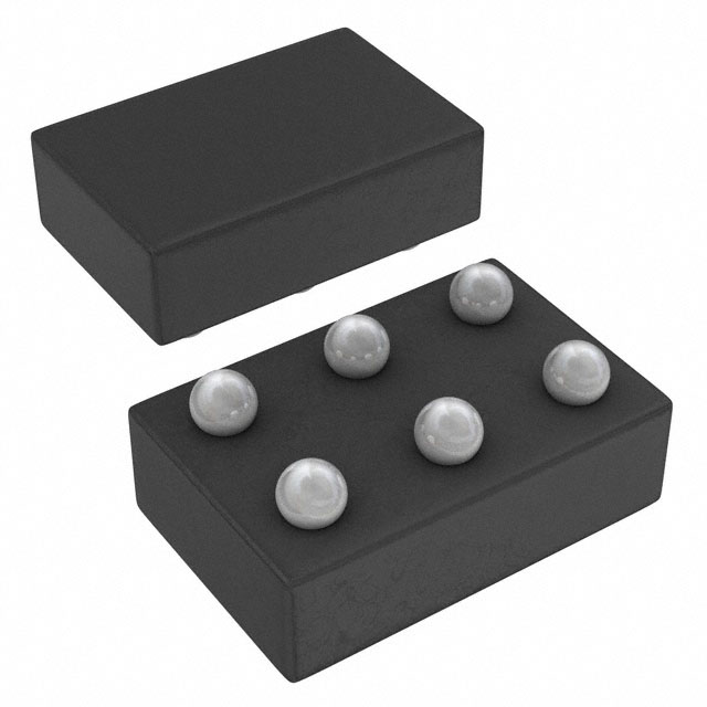
- Package: DSBGA (MicroStar Junior™), 6-Bump, 0.8 mm x 0.8 mm
- Essence: High-speed CMOS technology
- Packaging/Quantity: Tape and Reel, 3000 units per reel
Specifications
- Supply Voltage Range: 0.8 V to 3.6 V
- Input Voltage Range: 0 V to VCC + 0.5 V
- Output Voltage Range: 0 V to VCC + 0.5 V
- Operating Temperature Range: -40°C to +85°C
- Propagation Delay: 2.9 ns (typical)
- Maximum Frequency: 400 MHz
Detailed Pin Configuration
The SN74AUP1G57YFPR has the following pin configuration:
____
   A1 |    | VCC
   B1 |    | Y1
 GND1 |    | S1
   B2 |    | Y2
 GND2 |____| S2
Functional Features
The SN74AUP1G57YFPR is a single 2-input multiplexer that allows selection between two input signals (A and B) based on the select signal (S). It operates using high-speed CMOS technology, making it suitable for applications requiring fast switching times.
Advantages and Disadvantages
Advantages: - High-speed operation - Low power consumption - Small package size - Wide supply voltage range
Disadvantages: - Limited number of inputs and outputs - Not suitable for complex logic functions
Working Principles
The SN74AUP1G57YFPR works by using a combination of transistors and logic gates to control the flow of signals. When the select signal (S) is low, the output (Y1) follows input A. Conversely, when the select signal is high, the output (Y2) follows input B. This allows for flexible signal routing in various digital circuits.
Detailed Application Field Plans
The SN74AUP1G57YFPR can be used in a wide range of applications, including but not limited to: - Data multiplexing - Signal routing and switching - Logic level conversion - Communication systems - Consumer electronics - Industrial automation
Detailed and Complete Alternative Models
Some alternative models that can be considered as alternatives to the SN74AUP1G57YFPR are:
- SN74LVC1G57DBVR: Single 2-input Multiplexer, SOT-23 package, 5-pin configuration.
- MC74VHC1G57DTT1G: Single 2-input Multiplexer, SOT-23-5 package, 5-pin configuration.
- CD74HCT157M96: Quad 2-input Multiplexer, SOIC-16 package, 16-pin configuration.
These alternative models offer similar functionality and can be used as replacements depending on specific requirements.
In conclusion, the SN74AUP1G57YFPR is a single 2-input multiplexer IC with high-speed operation, low power consumption, and a small package size. It finds applications in various fields such as data multiplexing, signal routing, and logic level conversion. Alternative models provide flexibility based on specific needs.
Sebutkan 10 pertanyaan dan jawaban umum terkait penerapan SN74AUP1G57YFPR dalam solusi teknis
Sure! Here are 10 common questions and answers related to the application of SN74AUP1G57YFPR:
Q1: What is SN74AUP1G57YFPR? A1: SN74AUP1G57YFPR is a single configurable multiple-function gate that can be used in various technical solutions.
Q2: What are the key features of SN74AUP1G57YFPR? A2: Some key features include low power consumption, wide operating voltage range, and compatibility with different logic families.
Q3: What are the typical applications of SN74AUP1G57YFPR? A3: SN74AUP1G57YFPR can be used in signal switching, level shifting, multiplexing, and other similar applications.
Q4: What is the operating voltage range of SN74AUP1G57YFPR? A4: The operating voltage range is typically between 0.8V and 3.6V.
Q5: Can SN74AUP1G57YFPR be used with other logic families? A5: Yes, SN74AUP1G57YFPR is compatible with various logic families such as CMOS, TTL, and LVCMOS.
Q6: Does SN74AUP1G57YFPR have any built-in protection features? A6: Yes, it has built-in ESD (electrostatic discharge) protection to prevent damage from static electricity.
Q7: What is the maximum output current of SN74AUP1G57YFPR? A7: The maximum output current is typically around 32mA.
Q8: Can SN74AUP1G57YFPR operate at high frequencies? A8: Yes, it can operate at high frequencies, typically up to several hundred megahertz.
Q9: Is SN74AUP1G57YFPR available in different package options? A9: Yes, it is available in various package options such as SOT-23 and DSBGA.
Q10: Where can I find more information about the application of SN74AUP1G57YFPR? A10: You can refer to the datasheet provided by the manufacturer or visit their official website for detailed application notes and examples.
Please note that the answers provided here are general and may vary depending on specific requirements and use cases.