

Lihat spesifikasi untuk detail produk.
SN74AUC2G125YZPR
Product Overview
Category
The SN74AUC2G125YZPR belongs to the category of integrated circuits (ICs).
Use
This IC is commonly used for signal buffering and level shifting applications.
Characteristics
- Low power consumption
- High-speed operation
- Wide operating voltage range
- Small package size
- RoHS compliant
Package
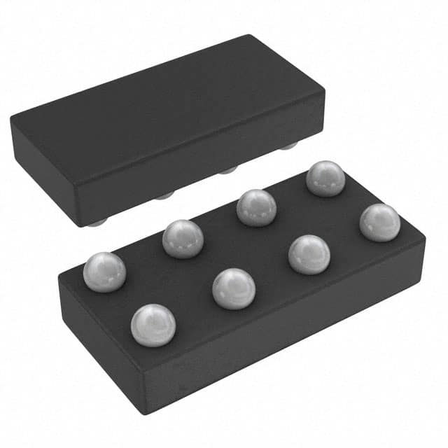
The SN74AUC2G125YZPR is available in a small outline package (SOP) with a pin count of 8.
Essence
The essence of this product lies in its ability to provide reliable signal buffering and level shifting capabilities in various electronic systems.
Packaging/Quantity
The SN74AUC2G125YZPR is typically packaged in reels, with each reel containing a specific quantity of ICs. The exact quantity may vary depending on the manufacturer's specifications.
Specifications
- Supply Voltage: 1.65V to 5.5V
- Operating Temperature Range: -40°C to +85°C
- Input Capacitance: 3.5pF (typical)
- Output Capacitance: 4.5pF (typical)
- Propagation Delay: 2.7ns (typical)
Detailed Pin Configuration
The SN74AUC2G125YZPR has the following pin configuration:
```
| | --| A Yn |-- --| B OE |-- --| GND A |-- --| VCC B |-- |___________| ```
Functional Features
- Dual buffer gates
- Non-inverting outputs
- Output enable control
- High-speed data transmission
- Low power consumption
Advantages and Disadvantages
Advantages
- Low power consumption makes it suitable for battery-powered devices.
- High-speed operation enables efficient data transmission.
- Wide operating voltage range allows compatibility with various systems.
- Small package size saves board space.
Disadvantages
- Limited number of buffer gates in a single IC.
- May not be suitable for applications requiring a large number of buffer gates.
Working Principles
The SN74AUC2G125YZPR operates by receiving input signals and buffering them to provide stable and reliable output signals. The non-inverting outputs ensure that the output signal matches the input signal polarity. The output enable control allows the user to enable or disable the output as required.
Detailed Application Field Plans
The SN74AUC2G125YZPR finds applications in various electronic systems, including but not limited to:
- Communication devices: Used for level shifting and buffering signals in communication systems such as routers, modems, and switches.
- Industrial automation: Enables signal buffering and level shifting in industrial control systems, PLCs, and motor drives.
- Consumer electronics: Utilized in devices like smartphones, tablets, and gaming consoles for signal conditioning and level shifting.
- Automotive electronics: Provides signal buffering and level shifting capabilities in automotive applications such as infotainment systems and engine control units.
Detailed and Complete Alternative Models
- SN74AUC2G125DCTR
- SN74AUC2G125DBVR
- SN74AUC2G125DCUR
- SN74AUC2G125DRLR
- SN74AUC2G125DCTRG4
These alternative models offer similar functionality and characteristics to the SN74AUC2G125YZPR, providing options for different package types and quantities.
In conclusion, the SN74AUC2G125YZPR is a versatile integrated circuit that offers reliable signal buffering and level shifting capabilities. Its low power consumption, high-speed operation, and small package size make it suitable for various applications in communication, industrial automation, consumer electronics, and automotive electronics.
Sebutkan 10 pertanyaan dan jawaban umum terkait penerapan SN74AUC2G125YZPR dalam solusi teknis
Sure! Here are 10 common questions and answers related to the application of SN74AUC2G125YZPR in technical solutions:
Q: What is SN74AUC2G125YZPR? A: SN74AUC2G125YZPR is a dual bus buffer gate with 3-state outputs, designed for low-voltage and low-power applications.
Q: What is the operating voltage range of SN74AUC2G125YZPR? A: The operating voltage range of SN74AUC2G125YZPR is from 0.8V to 3.6V.
Q: What is the maximum output current of SN74AUC2G125YZPR? A: The maximum output current of SN74AUC2G125YZPR is typically 24mA.
Q: Can SN74AUC2G125YZPR be used as a level shifter? A: Yes, SN74AUC2G125YZPR can be used as a level shifter to convert signals between different voltage levels.
Q: What is the propagation delay of SN74AUC2G125YZPR? A: The propagation delay of SN74AUC2G125YZPR is typically around 2.7ns.
Q: Is SN74AUC2G125YZPR suitable for high-speed applications? A: Yes, SN74AUC2G125YZPR is designed for high-speed operation and can be used in applications with fast switching requirements.
Q: Can SN74AUC2G125YZPR drive capacitive loads? A: Yes, SN74AUC2G125YZPR can drive small capacitive loads up to a certain limit specified in the datasheet.
Q: Does SN74AUC2G125YZPR have built-in ESD protection? A: Yes, SN74AUC2G125YZPR has built-in ESD protection to safeguard against electrostatic discharge events.
Q: Can SN74AUC2G125YZPR be used in battery-powered applications? A: Yes, SN74AUC2G125YZPR is suitable for battery-powered applications due to its low-voltage and low-power characteristics.
Q: What package options are available for SN74AUC2G125YZPR? A: SN74AUC2G125YZPR is available in various package options, such as the 8-pin VSSOP and DSBGA packages.
Please note that these answers are general and it's always recommended to refer to the datasheet and consult with technical experts for specific application requirements.