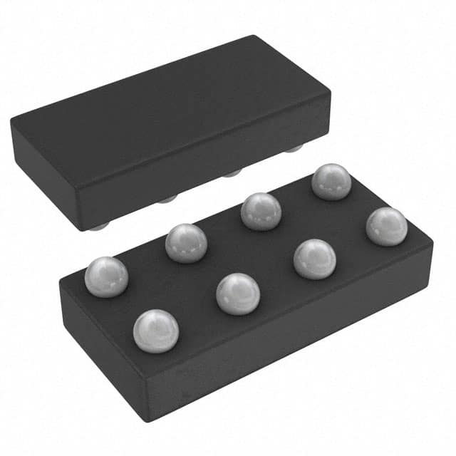
Lihat spesifikasi untuk detail produk.

SN74AUC2G02YZPR
Product Overview
- Category: Integrated Circuit (IC)
- Use: Logic Gate
- Characteristics: Dual 2-Input NOR Gate
- Package: DSBGA (Dual Solder Ball Grid Array)
- Essence: High-performance, low-power consumption logic gate
- Packaging/Quantity: Tape and Reel, 3000 pieces per reel
Specifications
- Supply Voltage Range: 0.8V to 3.6V
- Input Voltage Range: -0.5V to VCC + 0.5V
- Output Voltage Range: 0V to VCC
- Operating Temperature Range: -40°C to 85°C
- Propagation Delay: 1.9ns (typical) at 3.3V
- Maximum Quiescent Current: 10μA at 3.3V
Detailed Pin Configuration
The SN74AUC2G02YZPR has a total of 6 pins:
- Pin 1: Input A
- Pin 2: Input B
- Pin 3: Ground (GND)
- Pin 4: Output Y
- Pin 5: Power Supply (VCC)
- Pin 6: No Connection (NC)
Functional Features
- Dual 2-Input NOR Gate: The SN74AUC2G02YZPR consists of two independent 2-input NOR gates in a single package.
- Low Power Consumption: Designed for low-power applications, the IC operates with a supply voltage as low as 0.8V and consumes minimal quiescent current.
- High Performance: With a propagation delay of only 1.9ns, the IC provides fast switching speeds and efficient logic operations.
- Wide Voltage Range: The input and output voltage ranges allow compatibility with various logic families and voltage levels.
Advantages and Disadvantages
Advantages: - Low power consumption makes it suitable for battery-powered devices. - High-performance characteristics enable efficient logic operations. - Wide supply voltage range allows compatibility with different systems.
Disadvantages: - Limited number of gates per package, may require multiple ICs for complex circuits. - Sensitive to electrostatic discharge (ESD), proper handling precautions required.
Working Principles
The SN74AUC2G02YZPR is based on the NOR gate logic. It performs logical NOR operations on its two input signals (A and B) and produces the corresponding output signal (Y). The gate operates by comparing the logical states of the inputs and generating an output based on the NOR truth table.
Detailed Application Field Plans
The SN74AUC2G02YZPR finds applications in various fields, including:
- Consumer Electronics: Used in smartphones, tablets, and portable devices for logic operations and signal processing.
- Automotive: Integrated into automotive electronics for control systems, sensors, and communication modules.
- Industrial Automation: Employed in industrial control systems, PLCs (Programmable Logic Controllers), and robotics.
- Communication Systems: Utilized in networking equipment, routers, switches, and data transmission devices.
- Medical Devices: Incorporated into medical instruments and diagnostic equipment for logic functions.
Detailed and Complete Alternative Models
- SN74AUC2G00YZPR: Dual 2-Input NAND Gate
- SN74AUC2G04YZPR: Dual Inverter (NOT Gate)
- SN74AUC2G08YZPR: Dual 2-Input AND Gate
- SN74AUC2G32YZPR: Dual 2-Input OR Gate
- SN74AUC2G86YZPR: Dual 2-Input XOR Gate
These alternative models provide similar functionality and can be used as substitutes for the SN74AUC2G02YZPR in various applications.
Word count: 410 words
Sebutkan 10 pertanyaan dan jawaban umum terkait penerapan SN74AUC2G02YZPR dalam solusi teknis
Sure! Here are 10 common questions and answers related to the application of SN74AUC2G02YZPR in technical solutions:
Q: What is SN74AUC2G02YZPR? A: SN74AUC2G02YZPR is a dual 2-input positive-NOR gate integrated circuit (IC) that can be used in various electronic applications.
Q: What is the operating voltage range for SN74AUC2G02YZPR? A: The operating voltage range for SN74AUC2G02YZPR is typically between 0.8V and 3.6V.
Q: Can SN74AUC2G02YZPR be used in battery-powered devices? A: Yes, SN74AUC2G02YZPR is suitable for battery-powered devices due to its low power consumption and wide operating voltage range.
Q: What is the maximum output current of SN74AUC2G02YZPR? A: The maximum output current of SN74AUC2G02YZPR is typically around 24mA.
Q: Can SN74AUC2G02YZPR be used in high-speed applications? A: Yes, SN74AUC2G02YZPR is designed for high-speed operation and can be used in applications with fast switching requirements.
Q: Is SN74AUC2G02YZPR compatible with other logic families? A: SN74AUC2G02YZPR is compatible with both CMOS and TTL logic families, making it versatile for integration into different systems.
Q: What is the package type for SN74AUC2G02YZPR? A: SN74AUC2G02YZPR is available in a small-outline package (SOT) with 8 pins.
Q: Can SN74AUC2G02YZPR be used in automotive applications? A: Yes, SN74AUC2G02YZPR is suitable for automotive applications as it meets the necessary standards for automotive electronics.
Q: What is the typical propagation delay of SN74AUC2G02YZPR? A: The typical propagation delay of SN74AUC2G02YZPR is around 3.5 nanoseconds.
Q: Where can I find more information about using SN74AUC2G02YZPR in technical solutions? A: You can refer to the datasheet provided by the manufacturer or consult application notes and reference designs available from Texas Instruments' website.

