

Lihat spesifikasi untuk detail produk.
SN74AUC07RGYRG4
Product Overview
- Category: Integrated Circuit (IC)
- Use: Buffer/Driver
- Characteristics: High-speed, low-power, open-drain output
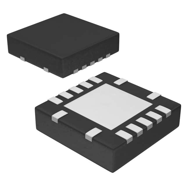
- Package: VQFN-14
- Essence: Hex buffer/driver with open-drain outputs
- Packaging/Quantity: Tape and reel, 2500 units per reel
Specifications
- Supply Voltage Range: 0.8V to 3.6V
- Input Voltage Range: -0.5V to 5.5V
- Output Voltage Range: 0V to VCC
- Maximum Operating Frequency: 500MHz
- Maximum Propagation Delay: 2.9ns
- Maximum Quiescent Current: 1μA
Detailed Pin Configuration
The SN74AUC07RGYRG4 has a VQFN-14 package with the following pin configuration:
__    __
   A1 | 1    14 | VCC
   A2 | 2    13 | Y1
   A3 | 3    12 | Y2
   A4 | 4    11 | Y3
   A5 | 5    10 | GND
   A6 | 6     9 | Y4
  GND | 7     8 | Y5
       ‾‾    ‾‾
Functional Features
- Hex buffer/driver with open-drain outputs
- Compatible with various logic families
- Low power consumption
- High-speed operation
- Wide supply voltage range
- ESD protection on all inputs and outputs
Advantages and Disadvantages
Advantages: - Versatile compatibility with different logic families - Low power consumption for energy-efficient applications - High-speed operation for time-critical tasks - Wide supply voltage range allows for flexibility in power sources - ESD protection ensures robustness and reliability
Disadvantages: - Limited number of buffer/driver outputs (6 in this case) - Open-drain outputs may require additional pull-up resistors in certain applications
Working Principles
The SN74AUC07RGYRG4 is a hex buffer/driver with open-drain outputs. It acts as an interface between different logic families, providing signal buffering and driving capabilities. The open-drain outputs allow for easy connection to other devices or circuits, as they can be pulled up to the desired voltage level externally.
When an input signal is received, the buffer amplifies it and drives the corresponding output pin. The open-drain configuration enables bidirectional communication and facilitates wired-OR connections. The device operates within a wide supply voltage range, making it suitable for various applications.
Detailed Application Field Plans
The SN74AUC07RGYRG4 finds applications in various fields, including:
- Communication Systems: Used for level shifting and signal buffering in data transmission systems.
- Industrial Automation: Enables interfacing between different control systems and sensors/actuators.
- Automotive Electronics: Provides signal conditioning and driving capabilities in automotive modules.
- Consumer Electronics: Used in audio/video equipment, gaming consoles, and home automation systems.
- Medical Devices: Facilitates signal amplification and isolation in medical monitoring equipment.
Detailed and Complete Alternative Models
- SN74AUP07RGYR: Similar to SN74AUC07RGYRG4 but operates at higher voltage levels (1.8V to 3.6V).
- SN74LVC07ARGYR: Low-voltage version with similar functionality and characteristics (1.65V to 3.6V).
- SN74LV1T07DBVR: Single buffer/driver with open-drain output and smaller package (SOT-23-5).
These alternative models offer similar functionality but may have different voltage ranges, package sizes, or pin configurations to suit specific application requirements.
Word count: 431 words
Sebutkan 10 pertanyaan dan jawaban umum terkait penerapan SN74AUC07RGYRG4 dalam solusi teknis
Sure! Here are 10 common questions and answers related to the application of SN74AUC07RGYRG4 in technical solutions:
Q: What is SN74AUC07RGYRG4? A: SN74AUC07RGYRG4 is a hex buffer/driver IC (integrated circuit) that provides high-performance, low-power buffering and driving capabilities.
Q: What is the voltage supply range for SN74AUC07RGYRG4? A: The voltage supply range for SN74AUC07RGYRG4 is typically between 0.8V and 3.6V.
Q: What is the maximum output current of SN74AUC07RGYRG4? A: SN74AUC07RGYRG4 can provide a maximum output current of 24mA per channel.
Q: Can SN74AUC07RGYRG4 be used for level shifting applications? A: Yes, SN74AUC07RGYRG4 can be used for level shifting as it supports both 3.3V and 5V logic levels.
Q: What is the typical propagation delay of SN74AUC07RGYRG4? A: The typical propagation delay of SN74AUC07RGYRG4 is around 2.7ns.
Q: Is SN74AUC07RGYRG4 suitable for high-speed data transmission? A: Yes, SN74AUC07RGYRG4 is designed for high-speed operation and can be used in applications requiring fast data transmission.
Q: Can SN74AUC07RGYRG4 drive capacitive loads? A: Yes, SN74AUC07RGYRG4 has a strong output drive capability and can drive capacitive loads up to 50pF.
Q: Does SN74AUC07RGYRG4 have built-in protection features? A: Yes, SN74AUC07RGYRG4 has built-in ESD (electrostatic discharge) protection on its inputs and outputs.
Q: Can SN74AUC07RGYRG4 be used in automotive applications? A: Yes, SN74AUC07RGYRG4 is qualified for automotive applications and meets the necessary standards.
Q: What package options are available for SN74AUC07RGYRG4? A: SN74AUC07RGYRG4 is available in various package options, including VQFN and SOIC packages.
Please note that these answers are general and may vary depending on specific datasheet specifications and application requirements.