

Lihat spesifikasi untuk detail produk.
SN74AUC06RGYR
Product Overview
- Category: Integrated Circuit (IC)
- Use: Inverting Buffer/Driver
- Characteristics:
- Low-voltage CMOS technology
- High-speed operation
- Wide operating voltage range
- Low power consumption
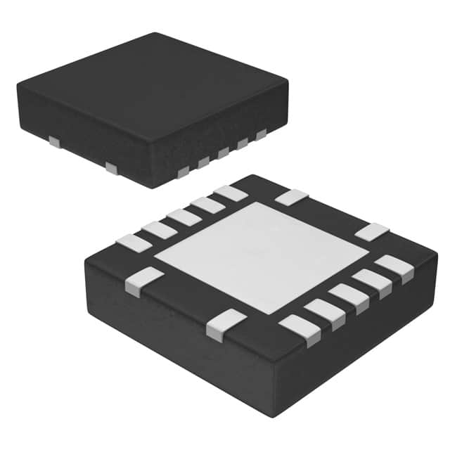
- Package: VQFN-14
- Essence: This IC is designed to provide high-performance buffering and driving capabilities in various electronic circuits.
- Packaging/Quantity: Tape and Reel, 2500 units per reel
Specifications
- Supply Voltage Range: 0.8V to 3.6V
- Input Voltage Range: 0V to VCC
- Output Voltage Range: 0V to VCC
- Maximum Operating Frequency: 100 MHz
- Propagation Delay: 2.5 ns (typical)
- Output Drive Capability: ±24 mA
- Operating Temperature Range: -40°C to +85°C
Detailed Pin Configuration
The SN74AUC06RGYR has a VQFN-14 package with the following pin configuration:
- A Input
- Y Output
- GND (Ground)
- A Input
- Y Output
- GND (Ground)
- A Input
- Y Output
- GND (Ground)
- A Input
- Y Output
- VCC (Supply Voltage)
- A Input
- Y Output
Functional Features
- Inverting Buffer/Driver: The SN74AUC06RGYR provides six independent inverting buffer/driver channels.
- High-Speed Operation: With a maximum operating frequency of 100 MHz, this IC ensures fast signal propagation.
- Wide Operating Voltage Range: It can operate within a wide supply voltage range of 0.8V to 3.6V, making it suitable for various applications.
- Low Power Consumption: The IC is designed to consume minimal power, enhancing energy efficiency in electronic systems.
Advantages and Disadvantages
Advantages: - High-speed operation enables quick signal processing. - Wide operating voltage range allows compatibility with different voltage levels. - Low power consumption helps conserve energy. - Small package size saves board space.
Disadvantages: - Limited output drive capability may not be suitable for high-current applications. - Propagation delay of 2.5 ns (typical) may impact timing-sensitive circuits.
Working Principles
The SN74AUC06RGYR operates based on low-voltage CMOS technology. It utilizes a combination of transistors and logic gates to invert and amplify input signals. When an input signal is applied, the IC processes it and produces the inverted output signal. The low-voltage design ensures efficient operation while minimizing power consumption.
Detailed Application Field Plans
The SN74AUC06RGYR finds applications in various electronic systems, including but not limited to: 1. Communication devices 2. Computer peripherals 3. Consumer electronics 4. Industrial automation 5. Automotive electronics
In communication devices, this IC can be used for level shifting, signal buffering, and driving applications. In computer peripherals, it can be employed for data transmission and interfacing purposes. In consumer electronics, it can assist in audio/video signal processing and control circuitry. In industrial automation, it can be utilized for sensor interfacing and control signal generation. In automotive electronics, it can contribute to signal conditioning and control modules.
Detailed and Complete Alternative Models
- SN74AUP06RGYR
- SN74LVC06ARGYR
- SN74LVU04ARGYR
- SN74HCU04ARGYR
- SN74HC06ARGYR
These alternative models offer similar functionality and characteristics to the SN74AUC06RGYR, providing options for different design requirements.
Word count: 480 words
Sebutkan 10 pertanyaan dan jawaban umum terkait penerapan SN74AUC06RGYR dalam solusi teknis
Sure! Here are 10 common questions and answers related to the application of SN74AUC06RGYR in technical solutions:
Q: What is SN74AUC06RGYR? A: SN74AUC06RGYR is a hex inverter buffer/driver with open-drain outputs, commonly used in digital logic circuits.
Q: What is the operating voltage range for SN74AUC06RGYR? A: The operating voltage range for SN74AUC06RGYR is typically between 0.8V and 3.6V.
Q: What is the maximum output current of SN74AUC06RGYR? A: The maximum output current of SN74AUC06RGYR is typically around 24mA.
Q: Can SN74AUC06RGYR be used as a level shifter? A: Yes, SN74AUC06RGYR can be used as a level shifter to convert signals between different voltage levels.
Q: Does SN74AUC06RGYR have internal pull-up or pull-down resistors? A: No, SN74AUC06RGYR does not have internal pull-up or pull-down resistors. External resistors may be required for specific applications.
Q: What is the propagation delay of SN74AUC06RGYR? A: The propagation delay of SN74AUC06RGYR is typically around 2.5ns.
Q: Can SN74AUC06RGYR drive capacitive loads directly? A: Yes, SN74AUC06RGYR can drive small capacitive loads directly without requiring additional buffering.
Q: Is SN74AUC06RGYR suitable for high-speed applications? A: Yes, SN74AUC06RGYR is designed for high-speed operation and can be used in applications with fast switching requirements.
Q: Can SN74AUC06RGYR tolerate overvoltage conditions? A: SN74AUC06RGYR has built-in protection features that allow it to tolerate limited overvoltage conditions, but exceeding the absolute maximum ratings should be avoided.
Q: Are there any specific layout considerations for using SN74AUC06RGYR? A: It is recommended to follow the manufacturer's guidelines for PCB layout, including proper decoupling capacitors and minimizing trace lengths to reduce noise and ensure reliable operation.
Please note that these answers are general and may vary depending on the specific application and operating conditions. It is always advisable to refer to the datasheet and consult with the manufacturer for detailed information.