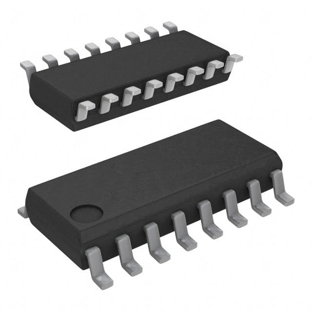
Lihat spesifikasi untuk detail produk.

SN74AS253AD
Product Overview
- Category: Integrated Circuit (IC)
- Use: Logic Multiplexer/Demultiplexer
- Characteristics: High-speed, low-power consumption
- Package: Dual In-Line Package (DIP)
- Essence: Combines two 4-input multiplexers and two 1-of-4 decoders in a single chip
- Packaging/Quantity: Available in tubes of 25 or reels of 2,000
Specifications
- Supply Voltage Range: 4.5V to 5.5V
- Input Voltage Range: 0V to VCC
- Operating Temperature Range: -40°C to +85°C
- Propagation Delay Time: 9ns (typical)
- Output Current: ±24mA
- Pin Count: 16
Detailed Pin Configuration
The SN74AS253AD has 16 pins arranged as follows:
__    __
   A1 -| 1    16 |- VCC
   A2 -| 2    15 |- B1
   A3 -| 3    14 |- B2
   A4 -| 4    13 |- Y1
   G1 -| 5    12 |- Y2
   G2 -| 6    11 |- Y3
   D1 -| 7    10 |- Y4
   D2 -| 8     9 |- GND
        ¯¯    ¯¯
Functional Features
- Combines two 4-input multiplexers and two 1-of-4 decoders
- Allows selection between two sets of four inputs using the common select inputs (A1-A4)
- Generates four outputs (Y1-Y4) based on the selected inputs
- Enables individual output selection using the enable inputs (G1, G2)
- High-speed operation suitable for time-critical applications
- Low-power consumption for energy-efficient designs
Advantages and Disadvantages
Advantages: - Integration of multiple functions in a single chip saves board space - High-speed operation allows for efficient data processing - Low-power consumption reduces energy requirements - Versatile functionality enables various applications
Disadvantages: - Limited number of inputs and outputs compared to more complex multiplexer/demultiplexer ICs - Requires careful consideration of input/output requirements for larger-scale projects
Working Principles
The SN74AS253AD operates by using the select inputs (A1-A4) to choose between two sets of four inputs. The selected inputs are then decoded by the internal circuitry to generate four corresponding outputs (Y1-Y4). The enable inputs (G1, G2) allow individual output selection, enabling flexibility in routing the desired signals.
Detailed Application Field Plans
The SN74AS253AD is commonly used in various digital systems where multiplexing or demultiplexing of signals is required. Some specific application fields include:
- Data Communication Systems: Used for signal routing and switching in data transmission networks.
- Industrial Automation: Enables efficient control and monitoring of industrial processes by selecting and routing sensor inputs.
- Test and Measurement Equipment: Facilitates signal selection and distribution in testing and measurement setups.
- Audio/Video Switching: Allows for seamless switching between different audio/video sources in entertainment systems.
- Computer Peripherals: Used in devices like printers and scanners for signal multiplexing/demultiplexing.
Detailed and Complete Alternative Models
- SN74AS253AN: Similar to SN74AS253AD but available in a different package (Plastic Dual In-Line Package).
- CD74HC253E: A CMOS version with similar functionality but operates at a lower voltage range (2V to 6V).
- MC74HC253N: Another CMOS alternative with comparable specifications and pin configuration.
These alternative models offer similar features and can be used as replacements depending on specific project requirements.
In conclusion, the SN74AS253AD is a versatile logic multiplexer/demultiplexer IC that combines two 4-input multiplexers and two 1-of-4 decoders in a single chip. Its high-speed operation, low-power consumption, and compact package make it suitable for various digital applications. However, its limited number of inputs and outputs should be considered for larger-scale projects. Alternative models like SN74AS253AN, CD74HC253E, and MC74HC253N provide options with similar functionality.
Sebutkan 10 pertanyaan dan jawaban umum terkait penerapan SN74AS253AD dalam solusi teknis
Sure! Here are 10 common questions and answers related to the application of SN74AS253AD:
Q: What is SN74AS253AD? A: SN74AS253AD is a dual 4-input multiplexer IC (Integrated Circuit) that can be used in various technical solutions.
Q: What is the purpose of SN74AS253AD? A: The purpose of SN74AS253AD is to select one of the four data inputs based on the control inputs, allowing for data routing and selection in electronic circuits.
Q: What is the voltage range supported by SN74AS253AD? A: SN74AS253AD supports a voltage range of 4.5V to 5.5V.
Q: How many control inputs does SN74AS253AD have? A: SN74AS253AD has two control inputs, commonly referred to as "S0" and "S1".
Q: How many data inputs can SN74AS253AD handle? A: SN74AS253AD can handle four data inputs, labeled as "A0", "A1", "B0", and "B1".
Q: How many output pins does SN74AS253AD have? A: SN74AS253AD has two output pins, typically labeled as "Y0" and "Y1".
Q: What is the function of the output pins in SN74AS253AD? A: The output pins in SN74AS253AD provide the selected data output based on the control inputs.
Q: Can SN74AS253AD be cascaded to increase the number of inputs? A: Yes, SN74AS253AD can be cascaded to increase the number of inputs by connecting the output of one IC to the input of another.
Q: What is the maximum operating frequency of SN74AS253AD? A: The maximum operating frequency of SN74AS253AD is typically around 125 MHz.
Q: In what types of applications can SN74AS253AD be used? A: SN74AS253AD can be used in various applications such as data routing, signal selection, multiplexing, and digital circuit design.
Please note that these answers are general and may vary depending on specific use cases and requirements.

