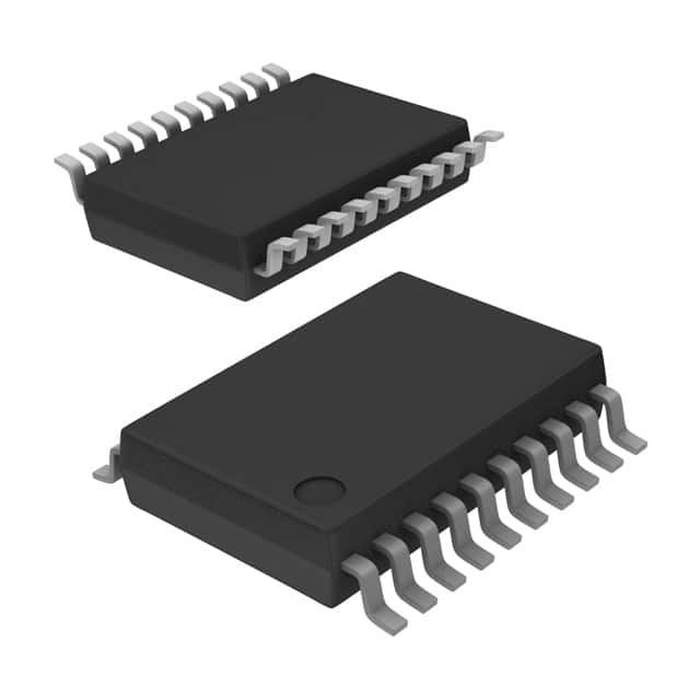
Lihat spesifikasi untuk detail produk.

SN74ALS541DBRG4
Product Overview
- Category: Integrated Circuit (IC)
- Use: Buffer/Line Driver
- Characteristics: High-speed, low-power, TTL-compatible
- Package: SOIC (Small Outline Integrated Circuit)
- Essence: Logic gate with 8-bit tri-state buffer
- Packaging/Quantity: Tape and Reel, 2500 units per reel
Specifications
- Supply Voltage Range: 4.5V to 5.5V
- Input Voltage Range: 0V to VCC
- Output Voltage Range: 0V to VCC
- Operating Temperature Range: -40°C to +85°C
- Propagation Delay Time: 6ns (typical)
- Output Current: ±24mA
- Input Capacitance: 3pF
- Output Capacitance: 15pF
Detailed Pin Configuration
The SN74ALS541DBRG4 has a total of 20 pins, which are arranged as follows:
- OE (Output Enable) - Active Low
- A1 (Input A1)
- Y1 (Output Y1)
- A2 (Input A2)
- Y2 (Output Y2)
- A3 (Input A3)
- Y3 (Output Y3)
- GND (Ground)
- Y4 (Output Y4)
- A4 (Input A4)
- Y5 (Output Y5)
- A5 (Input A5)
- Y6 (Output Y6)
- A6 (Input A6)
- Y7 (Output Y7)
- A7 (Input A7)
- Y8 (Output Y8)
- VCC (Supply Voltage)
- GND (Ground)
- OE (Output Enable) - Active Low
Functional Features
- 8-bit tri-state buffer with output enable control
- High-speed operation, suitable for applications requiring fast data transfer
- Low-power consumption, ideal for battery-powered devices
- TTL-compatible inputs and outputs, ensuring compatibility with a wide range of systems
- Tri-state outputs allow multiple devices to share a common bus without interference
Advantages and Disadvantages
Advantages: - High-speed operation enables efficient data transfer - Low-power consumption extends battery life in portable devices - TTL compatibility ensures easy integration into existing systems - Tri-state outputs facilitate bus sharing in multi-device configurations
Disadvantages: - Limited voltage range (4.5V to 5.5V) may not be suitable for all applications - Propagation delay time of 6ns may introduce timing issues in certain high-speed applications
Working Principles
The SN74ALS541DBRG4 is a buffer/line driver IC that amplifies and controls the signals passing through it. It consists of eight independent tri-state buffers, each capable of driving one bit of data. The output enable (OE) pin controls the activation of the buffer outputs.
When the OE pin is low (active), the buffer outputs are enabled and can drive the connected circuitry. Conversely, when the OE pin is high (inactive), the buffer outputs are disabled and enter a high-impedance state, allowing other devices to drive the bus.
Detailed Application Field Plans
The SN74ALS541DBRG4 is commonly used in various applications, including:
- Data communication systems: It can be used to interface between different logic families or to amplify and buffer signals in data transmission lines.
- Microprocessor systems: It facilitates bus sharing and signal buffering in microcontroller-based systems.
- Memory systems: It helps in controlling and amplifying signals in memory address and data buses.
- Industrial automation: It is suitable for buffering and driving signals in control systems, PLCs (Programmable Logic Controllers), and motor control circuits.
Detailed and Complete Alternative Models
- SN74ALS540DBRG4: Similar to SN74ALS541DBRG4 but without the output enable control feature.
- SN74ALS244AN: Octal buffer/line driver with non-inverting outputs.
- SN74LS07N: Hex buffer/driver with open-collector outputs.
These alternative models offer similar functionality and can be used as substitutes depending on specific requirements.
Word count: 550 words
Sebutkan 10 pertanyaan dan jawaban umum terkait penerapan SN74ALS541DBRG4 dalam solusi teknis
Sure! Here are 10 common questions and answers related to the application of SN74ALS541DBRG4 in technical solutions:
Q: What is SN74ALS541DBRG4? A: SN74ALS541DBRG4 is a type of integrated circuit (IC) commonly used as a buffer or line driver in digital systems.
Q: What is the purpose of using SN74ALS541DBRG4 in a technical solution? A: SN74ALS541DBRG4 is used to amplify and buffer digital signals, ensuring proper signal integrity and driving capability.
Q: What voltage levels does SN74ALS541DBRG4 support? A: SN74ALS541DBRG4 supports a wide range of voltage levels, typically between 2V and 6V.
Q: Can SN74ALS541DBRG4 be used for bidirectional communication? A: No, SN74ALS541DBRG4 is unidirectional and can only be used for one-way signal transmission.
Q: How many channels does SN74ALS541DBRG4 have? A: SN74ALS541DBRG4 has 8 channels, allowing it to handle multiple signals simultaneously.
Q: What is the maximum current that SN74ALS541DBRG4 can drive? A: SN74ALS541DBRG4 can typically drive up to 24mA of current per channel.
Q: Is SN74ALS541DBRG4 compatible with TTL logic levels? A: Yes, SN74ALS541DBRG4 is compatible with both TTL and CMOS logic levels.
Q: Can SN74ALS541DBRG4 tolerate overvoltage conditions? A: SN74ALS541DBRG4 has built-in protection mechanisms to handle overvoltage conditions, but it is recommended to stay within the specified voltage range.
Q: What is the operating temperature range for SN74ALS541DBRG4? A: SN74ALS541DBRG4 can operate within a temperature range of -40°C to 85°C.
Q: Are there any specific layout considerations when using SN74ALS541DBRG4? A: Yes, it is important to follow the recommended layout guidelines provided in the datasheet to minimize noise and ensure proper signal integrity.
Please note that these answers are general and may vary depending on the specific application and requirements. It is always recommended to refer to the datasheet and consult with technical experts for accurate information.

