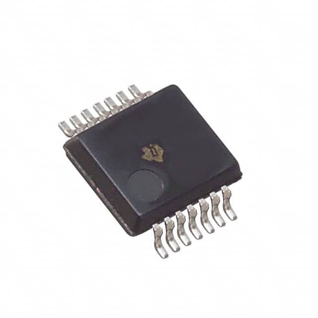
Lihat spesifikasi untuk detail produk.

SN74AHCT02DBR
Product Overview
- Category: Integrated Circuit (IC)
- Use: Logic Gate
- Characteristics: High-Speed, Low-Power, Quad 2-Input NOR Gate
- Package: SSOP (Shrink Small Outline Package)
- Essence: Digital Logic Component
- Packaging/Quantity: Tape and Reel, 2500 pieces per reel
Specifications
- Supply Voltage Range: 4.5V to 5.5V
- Input Voltage Range: 0V to VCC
- Output Voltage Range: 0V to VCC
- Operating Temperature Range: -40°C to +85°C
- Propagation Delay Time: 7 ns (typical)
- Quiescent Current: 1 µA (maximum)
Detailed Pin Configuration
The SN74AHCT02DBR has a total of 14 pins, which are assigned specific functions as follows:
- Pin 1: Input A1
- Pin 2: Input B1
- Pin 3: Output Y1
- Pin 4: Ground (GND)
- Pin 5: Input A2
- Pin 6: Input B2
- Pin 7: Output Y2
- Pin 8: VCC (Supply Voltage)
- Pin 9: Output Y3
- Pin 10: Input B3
- Pin 11: Input A3
- Pin 12: Output Y4
- Pin 13: Input B4
- Pin 14: Input A4
Functional Features
- Quad 2-Input NOR Gate: The SN74AHCT02DBR consists of four independent 2-input NOR gates, allowing for versatile logic operations.
- High-Speed Operation: With a propagation delay time of only 7 ns, this IC enables fast data processing.
- Low Power Consumption: The SN74AHCT02DBR is designed to operate at low power levels, making it suitable for battery-powered devices.
- Wide Operating Voltage Range: It can function within a supply voltage range of 4.5V to 5.5V, providing flexibility in various applications.
Advantages and Disadvantages
Advantages: - High-speed operation allows for efficient data processing. - Low power consumption makes it suitable for portable devices. - Versatile logic operations due to the presence of four independent NOR gates.
Disadvantages: - Limited to digital logic applications and cannot perform analog functions. - Requires proper handling and static discharge precautions due to its sensitivity to electrostatic discharge (ESD).
Working Principles
The SN74AHCT02DBR operates based on the principles of digital logic. Each NOR gate within the IC performs a logical NOR operation on its two input signals, producing an output signal based on the truth table of the NOR gate. The inputs and outputs are connected internally using transistors and other electronic components.
Detailed Application Field Plans
The SN74AHCT02DBR finds applications in various fields, including:
- Digital Electronics: Used in the design and implementation of digital circuits, such as arithmetic logic units (ALUs), multiplexers, and memory systems.
- Microcontrollers: Employed in microcontroller-based systems for performing logical operations and interfacing with other digital components.
- Communication Systems: Integrated into communication systems for signal processing, error detection, and correction.
- Industrial Automation: Utilized in control systems, PLCs (Programmable Logic Controllers), and robotics for logical decision-making and control.
Detailed and Complete Alternative Models
- SN74AHCT00DBR: Quad 2-Input NAND Gate
- SN74AHCT04DBR: Hex Inverter
- SN74AHCT08DBR: Quad 2-Input AND Gate
- SN74AHCT32DBR: Quad 2-Input OR Gate
- SN74AHCT86DBR: Quad 2-Input XOR Gate
These alternative models provide similar functionality to the SN74AHCT02DBR and can be used as substitutes depending on specific requirements.
Word count: 520 words
Sebutkan 10 pertanyaan dan jawaban umum terkait penerapan SN74AHCT02DBR dalam solusi teknis
Sure! Here are 10 common questions and answers related to the application of SN74AHCT02DBR:
Q: What is SN74AHCT02DBR? A: SN74AHCT02DBR is a quad 2-input NOR gate IC (integrated circuit) that is commonly used in digital logic circuits.
Q: What is the operating voltage range for SN74AHCT02DBR? A: The operating voltage range for SN74AHCT02DBR is typically between 4.5V and 5.5V.
Q: Can SN74AHCT02DBR be used in both CMOS and TTL logic systems? A: Yes, SN74AHCT02DBR is compatible with both CMOS and TTL logic systems.
Q: What is the maximum output current of SN74AHCT02DBR? A: The maximum output current of SN74AHCT02DBR is typically around 8mA.
Q: Can SN74AHCT02DBR be used as a level shifter? A: Yes, SN74AHCT02DBR can be used as a level shifter to convert signals between different voltage levels.
Q: What is the propagation delay of SN74AHCT02DBR? A: The propagation delay of SN74AHCT02DBR is typically around 7 ns.
Q: Can SN74AHCT02DBR be used in high-speed applications? A: Yes, SN74AHCT02DBR can be used in high-speed applications due to its fast switching speed.
Q: How many inputs does SN74AHCT02DBR have? A: SN74AHCT02DBR has four inputs, with two inputs per gate.
Q: Can SN74AHCT02DBR be used in both commercial and industrial applications? A: Yes, SN74AHCT02DBR is suitable for use in both commercial and industrial applications.
Q: Is SN74AHCT02DBR available in different package types? A: Yes, SN74AHCT02DBR is available in various package types, such as SOIC (Small Outline Integrated Circuit) and TSSOP (Thin Shrink Small Outline Package).
Please note that the answers provided here are general and may vary depending on specific datasheet specifications and application requirements.

