Lihat spesifikasi untuk detail produk.

SN74AHC367DGVRE4
Overview
Category: Integrated Circuit (IC)
Use: The SN74AHC367DGVRE4 is a high-speed hex buffer/driver with 3-state outputs. It is designed to drive capacitive loads while maintaining low power consumption and high speed operation.
Characteristics: - High-speed operation - Low power consumption - 3-state outputs - Wide operating voltage range - Schmitt-trigger inputs for noise immunity
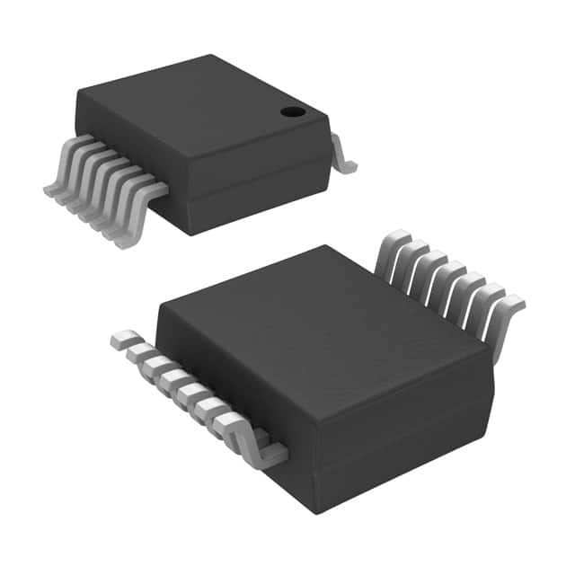
Package: VSSOP (Very Small Outline Package)
Essence: The SN74AHC367DGVRE4 is an essential component in electronic circuits that require buffering and driving capabilities. It ensures reliable signal transmission between different parts of a circuit.
Packaging/Quantity: The SN74AHC367DGVRE4 is typically sold in reels, with 2500 units per reel.
Specifications
- Supply Voltage Range: 2 V to 5.5 V
- Input Voltage Range: 0 V to VCC
- Output Voltage Range: 0 V to VCC
- Operating Temperature Range: -40°C to +85°C
- Maximum Propagation Delay: 6 ns
- Maximum Quiescent Current: 1 μA
Pin Configuration
The SN74AHC367DGVRE4 has a total of 16 pins. The pin configuration is as follows:
___________
   OE | 1       16 | VCC
  A1  | 2       15 | Y1
  A2  | 3       14 | Y2
  A3  | 4       13 | Y3
  A4  | 5       12 | Y4
  A5  | 6       11 | Y5
  A6  | 7       10 | Y6
 GND  | 8        9 | OE#
       ‾‾‾‾‾‾‾‾‾‾‾
Functional Features
- Hex buffer/driver with 3-state outputs
- High-speed operation allows for efficient signal transmission
- Low power consumption ensures energy efficiency
- Schmitt-trigger inputs provide noise immunity
- Wide operating voltage range allows for compatibility with various systems
Advantages and Disadvantages
Advantages: - High-speed operation enables fast data transfer - Low power consumption reduces energy usage - 3-state outputs allow for flexible signal control - Wide operating voltage range provides compatibility with different systems - Schmitt-trigger inputs enhance noise immunity
Disadvantages: - Limited number of output pins (6 in total) - May not be suitable for applications requiring a large number of buffered outputs
Working Principles
The SN74AHC367DGVRE4 operates by receiving input signals on its A1 to A6 pins. These signals are then buffered and amplified before being transmitted to the corresponding Y1 to Y6 output pins. The OE (Output Enable) pin controls the state of the outputs, allowing them to be either active or in a high-impedance state.
Detailed Application Field Plans
The SN74AHC367DGVRE4 is commonly used in various electronic applications, including:
- Data communication systems
- Microcontrollers and microprocessors
- Memory interfaces
- Industrial automation
- Automotive electronics
- Consumer electronics
In data communication systems, the SN74AHC367DGVRE4 can be used to buffer and drive signals between different components, ensuring reliable data transmission. In microcontrollers and microprocessors, it can be utilized to interface with external devices and peripherals. In memory interfaces, it helps in maintaining signal integrity during data transfer. In industrial automation and automotive electronics, it plays a crucial role in controlling and driving various components. In consumer electronics, it can be found in devices such as smartphones, tablets, and gaming consoles.
Detailed and Complete Alternative Models
- SN74AHC367DGVR
- SN74AHC367DGVRE4
- SN74AHC367DR
- SN74AHC367NSR
- SN74AHC367PWR
These alternative models offer similar functionality and characteristics to the SN74AHC367DGVRE4, providing options for different package types or quantities.
In conclusion, the SN74AHC367DGVRE4 is a high-speed hex buffer/driver with 3-state outputs. It offers advantages such as high-speed operation, low power consumption, and wide operating voltage range. However, it has a limited number of output pins and may not be suitable for applications requiring a large number of buffered outputs. It finds applications in various fields, including data communication systems, microcontrollers, memory interfaces, industrial automation,
Sebutkan 10 pertanyaan dan jawaban umum terkait penerapan SN74AHC367DGVRE4 dalam solusi teknis
Sure! Here are 10 common questions and answers related to the application of SN74AHC367DGVRE4 in technical solutions:
Q: What is the SN74AHC367DGVRE4? A: The SN74AHC367DGVRE4 is a hex buffer/driver with 3-state outputs, commonly used in digital logic applications.
Q: What is the voltage supply range for this IC? A: The SN74AHC367DGVRE4 operates with a voltage supply range of 2 V to 5.5 V.
Q: How many buffers/drivers are included in this IC? A: This IC contains six independent buffers/drivers.
Q: What is the maximum output current that each buffer/driver can handle? A: Each buffer/driver in the SN74AHC367DGVRE4 can handle a maximum output current of 8 mA.
Q: Can I connect multiple SN74AHC367DGVRE4 ICs together? A: Yes, you can connect multiple ICs together to expand the number of buffers/drivers available in your circuit.
Q: What is the typical propagation delay of this IC? A: The typical propagation delay of the SN74AHC367DGVRE4 is around 7 ns.
Q: Is this IC compatible with both TTL and CMOS logic levels? A: Yes, the SN74AHC367DGVRE4 is compatible with both TTL and CMOS logic levels.
Q: Can I use this IC for level shifting applications? A: Yes, this IC can be used for level shifting between different voltage domains.
Q: Does this IC have built-in protection features? A: Yes, the SN74AHC367DGVRE4 has built-in protection features like overvoltage and undervoltage lockout.
Q: What is the package type for this IC? A: The SN74AHC367DGVRE4 comes in a small SOT-23-8 package.
Please note that these answers are general and may vary depending on the specific application and requirements. It's always recommended to refer to the datasheet and consult with an expert for detailed information.

