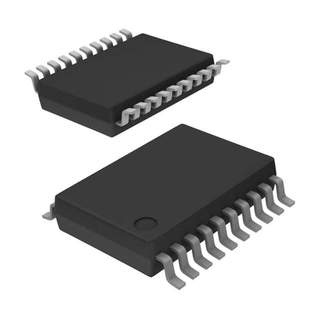
Lihat spesifikasi untuk detail produk.

SN74AC241DBR
Product Overview
Category
SN74AC241DBR belongs to the category of integrated circuits (ICs).
Use
This product is commonly used in electronic devices for signal amplification, buffering, and level shifting.
Characteristics
- High-speed operation
- Low power consumption
- Wide operating voltage range
- Compatibility with various logic families
Package
SN74AC241DBR is available in a small-outline integrated circuit (SOIC) package.
Essence
The essence of this product lies in its ability to provide reliable and efficient signal processing and manipulation.
Packaging/Quantity
SN74AC241DBR is typically packaged in reels, with each reel containing a specific quantity of ICs.
Specifications
- Supply Voltage: 2V - 6V
- Operating Temperature Range: -40°C to +85°C
- Input Voltage High Level (VIH): 2V - VCC
- Input Voltage Low Level (VIL): GND - 0.8V
- Output Voltage High Level (VOH): VCC - 0.5V
- Output Voltage Low Level (VOL): 0.4V
Detailed Pin Configuration
- A1: Input A1
- B1: Input B1
- GND: Ground
- A2: Input A2
- B2: Input B2
- Y2: Output Y2
- Y1: Output Y1
- OE: Output Enable
- VCC: Power Supply
Functional Features
- Eight input/output lines
- Non-inverting buffer
- Active-low output enable (OE) control
- High-speed operation
Advantages and Disadvantages
Advantages
- High-speed operation allows for efficient signal processing.
- Low power consumption helps in reducing energy usage.
- Wide operating voltage range ensures compatibility with various systems.
- Non-inverting buffer maintains signal integrity.
Disadvantages
- Limited number of input/output lines may restrict certain applications.
- Active-low output enable control may require additional circuitry for specific use cases.
Working Principles
SN74AC241DBR operates by receiving input signals through the A1, B1, A2, and B2 pins. These signals are then processed and amplified by the internal circuitry. The output signals, Y1 and Y2, can be controlled using the OE pin. When OE is low, the outputs are enabled, allowing the processed signals to pass through. Conversely, when OE is high, the outputs are disabled, effectively isolating the device from the external circuit.
Detailed Application Field Plans
SN74AC241DBR finds application in various electronic devices and systems, including: - Microcontrollers - Digital signal processors - Communication equipment - Industrial automation systems - Consumer electronics
Detailed and Complete Alternative Models
Some alternative models that offer similar functionality to SN74AC241DBR include: - SN74HC241DBR - SN74ACT241DBR - SN74LS241DBR - SN74LVC241DBR
These models differ in terms of voltage levels, speed, and other specifications. It is important to select the appropriate alternative based on the specific requirements of the application.
Word count: 442 words
Sebutkan 10 pertanyaan dan jawaban umum terkait penerapan SN74AC241DBR dalam solusi teknis
Sure! Here are 10 common questions and answers related to the application of SN74AC241DBR:
Question: What is SN74AC241DBR?
- Answer: SN74AC241DBR is a specific model of octal buffer and line driver integrated circuit (IC) manufactured by Texas Instruments.Question: What is the purpose of SN74AC241DBR?
- Answer: SN74AC241DBR is used to provide buffering and signal amplification for digital signals in various technical solutions.Question: What is the voltage range supported by SN74AC241DBR?
- Answer: SN74AC241DBR supports a voltage range of 2V to 6V.Question: How many input/output pins does SN74AC241DBR have?
- Answer: SN74AC241DBR has 8 input pins and 8 output pins, making it an octal buffer.Question: Can SN74AC241DBR handle bidirectional data flow?
- Answer: No, SN74AC241DBR is a unidirectional buffer and line driver, meaning it can only drive signals from inputs to outputs.Question: What is the maximum output current that SN74AC241DBR can provide?
- Answer: SN74AC241DBR can provide a maximum output current of 24mA per channel.Question: Is SN74AC241DBR compatible with TTL logic levels?
- Answer: Yes, SN74AC241DBR is compatible with both TTL and CMOS logic levels.Question: Can SN74AC241DBR be cascaded to increase the number of buffered outputs?
- Answer: Yes, multiple SN74AC241DBR ICs can be cascaded to increase the number of buffered outputs in a system.Question: What is the typical propagation delay of SN74AC241DBR?
- Answer: The typical propagation delay of SN74AC241DBR is around 5 nanoseconds.Question: Is SN74AC241DBR suitable for high-speed applications?
- Answer: Yes, SN74AC241DBR is designed for high-speed operation and can be used in various high-frequency applications.
Please note that these answers are general and may vary depending on specific application requirements.

