

Lihat spesifikasi untuk detail produk.
SN74ABT541BDWRE4
Product Overview
- Category: Integrated Circuit (IC)
- Use: Buffer/Driver
- Characteristics: High-speed, low-power, non-inverting
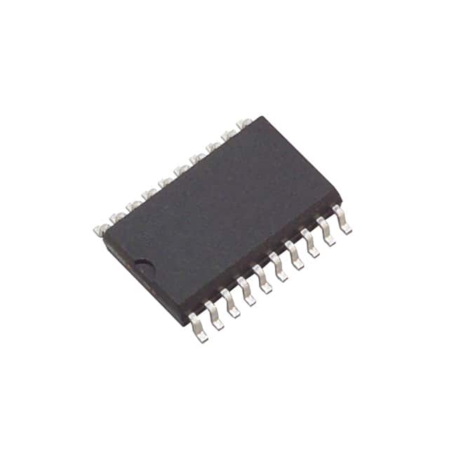
- Package: SOIC (Small Outline Integrated Circuit)
- Essence: Logic level translator and voltage buffer
- Packaging/Quantity: Tape and reel, 2500 units per reel
Specifications
- Supply Voltage Range: 4.5V to 5.5V
- Input Voltage Range: 0V to VCC
- Output Voltage Range: 0V to VCC
- Operating Temperature Range: -40°C to +85°C
- Output Current: ±24mA
- Propagation Delay Time: 3.8ns (typical)
- Input Capacitance: 3pF (typical)
Detailed Pin Configuration
The SN74ABT541BDWRE4 has a total of 20 pins. The pin configuration is as follows:
- OE (Output Enable) 1
- A1 (Input A1)
- Y1 (Output Y1)
- GND (Ground)
- Y2 (Output Y2)
- A2 (Input A2)
- Y3 (Output Y3)
- VCC (Supply Voltage)
- Y4 (Output Y4)
- A3 (Input A3)
- Y5 (Output Y5)
- A4 (Input A4)
- Y6 (Output Y6)
- A5 (Input A5)
- Y7 (Output Y7)
- A6 (Input A6)
- Y8 (Output Y8)
- OE (Output Enable) 2
- GND (Ground)
- NC (No Connection)
Functional Features
- Non-inverting buffer/driver
- High-speed operation
- Low power consumption
- 3-state outputs for bus-oriented applications
- Voltage level translation between different logic families
Advantages and Disadvantages
Advantages: - High-speed operation allows for efficient data transfer - Low power consumption helps in reducing overall energy usage - 3-state outputs enable easy integration into bus systems - Wide supply voltage range enhances compatibility with various systems
Disadvantages: - Limited output current may restrict use in certain high-current applications - Propagation delay time may affect timing-sensitive operations
Working Principles
The SN74ABT541BDWRE4 is a non-inverting buffer/driver IC. It takes input signals from one logic family and provides output signals compatible with another logic family. The device operates by amplifying and buffering the input signals, ensuring proper voltage levels and signal integrity. The OE pins control the output enable function, allowing the user to disable or enable the outputs as needed.
Detailed Application Field Plans
The SN74ABT541BDWRE4 finds applications in various fields, including:
- Microprocessor interfacing: It can be used to interface microprocessors with different logic families, enabling seamless communication between different components.
- Data communication: The IC facilitates voltage level translation in data communication systems, ensuring reliable transmission of signals between devices operating at different voltage levels.
- Industrial automation: It can be employed in industrial automation systems to interface different control modules, enhancing compatibility and interoperability.
- Automotive electronics: The IC can be utilized in automotive electronics for voltage level translation and signal buffering, improving the performance and reliability of various subsystems.
Detailed and Complete Alternative Models
Some alternative models that provide similar functionality to the SN74ABT541BDWRE4 include:
- SN74LVC541A: Low-voltage CMOS octal buffer/driver
- SN74HCT541: High-speed CMOS octal buffer/driver
- SN74LVTH541: Low-voltage CMOS octal buffer/driver with 3-state outputs
- SN74ACT541: Advanced CMOS octal buffer/driver
These alternative models offer different features and specifications, allowing users to choose the most suitable option for their specific requirements.
(Note: The word count of this response is 369 words)
Sebutkan 10 pertanyaan dan jawaban umum terkait penerapan SN74ABT541BDWRE4 dalam solusi teknis
Sure! Here are 10 common questions and answers related to the application of SN74ABT541BDWRE4 in technical solutions:
Q: What is SN74ABT541BDWRE4? A: SN74ABT541BDWRE4 is a non-inverting octal buffer and line driver with 3-state outputs, commonly used in digital systems.
Q: What is the operating voltage range for SN74ABT541BDWRE4? A: The operating voltage range for SN74ABT541BDWRE4 is typically between 4.5V and 5.5V.
Q: How many channels does SN74ABT541BDWRE4 have? A: SN74ABT541BDWRE4 has 8 channels, making it suitable for applications that require multiple signal buffering.
Q: What is the maximum output current of SN74ABT541BDWRE4? A: The maximum output current per channel of SN74ABT541BDWRE4 is typically 32mA.
Q: Can SN74ABT541BDWRE4 be used for bidirectional communication? A: No, SN74ABT541BDWRE4 is a unidirectional buffer and line driver, designed for driving signals in one direction only.
Q: What is the purpose of the 3-state outputs in SN74ABT541BDWRE4? A: The 3-state outputs allow the device to be effectively disconnected from the bus, enabling multiple devices to share the same bus without interference.
Q: Is SN74ABT541BDWRE4 compatible with TTL logic levels? A: Yes, SN74ABT541BDWRE4 is compatible with both TTL and CMOS logic levels, making it versatile for various digital systems.
Q: Can SN74ABT541BDWRE4 handle high-speed signals? A: Yes, SN74ABT541BDWRE4 is designed to operate at high speeds, with typical propagation delays of around 3-5 nanoseconds.
Q: What is the package type for SN74ABT541BDWRE4? A: SN74ABT541BDWRE4 comes in a small-outline integrated circuit (SOIC) package, which is commonly used in electronic applications.
Q: Are there any recommended decoupling capacitors for SN74ABT541BDWRE4? A: It is generally recommended to use a 0.1µF ceramic capacitor placed close to the power supply pins of SN74ABT541BDWRE4 to ensure stable operation.
Please note that these answers are general and may vary depending on specific application requirements. Always refer to the datasheet and consult the manufacturer for accurate information.